SK hynix’s Quality Design New Deal aims to develop optimized products with the world’s best quality and characteristics to secure a stable supply of highest quality DRAMs and provide better value to customers and employees. To achieve this, the company is building a system that enables continuous improvement of completeness and competitiveness through changes in product, technology, constitution, and culture. It is divided into four policies: Process New Deal, Platform New Deal, Digital New Deal, and Data New Deal.
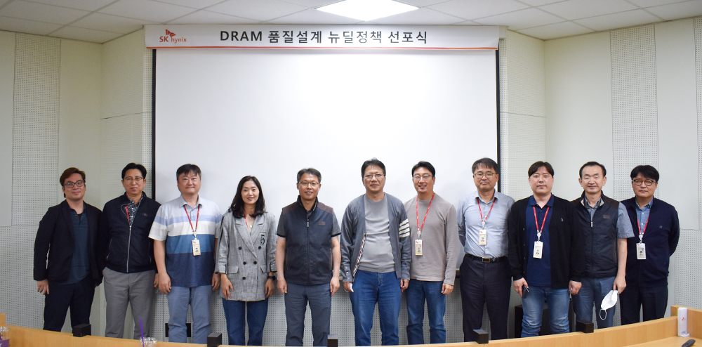
▲ Figure 1. Members of SK hynix DRAM Design Group at the Announcement Ceremony for the Quality Design New Deal
Building a System that Enables Continuous Improvement
F.D. Roosevelt, the 32nd President of the United States, implemented the New Deal as a plan to overcome the Great Depression. It laid the groundwork for the United States’ global dominance. In many ways, there seems to be little difference between the present ICT business environment and the chaos of the Great Depression.
The memory business model is becoming increasingly complex, diverse, and uncertain, requiring the rapid development of efficient and versatile products. SK hynix’s DRAM Design group has set out to promote the Quality Design New Deal policy to effectively respond to these requirements and innovatively improve its product development system.
The purpose of the Quality Design New Deal is to build a system that enables continuous improvement of completeness and competitiveness through changes in product, technology, constitution, and culture. It consists of the following four policies:
① Process New Deal: Securing a stable design work process to improve design completeness
② Platform New Deal: Preparing a technology development system to secure the best technology, and securing the continuity of technology
③ Digital New Deal: Changing the constitution of ‘analog → digital’ to improve development efficiency and productivity
④ Data New Deal: Establishing data-based decision making and AI-based design environment
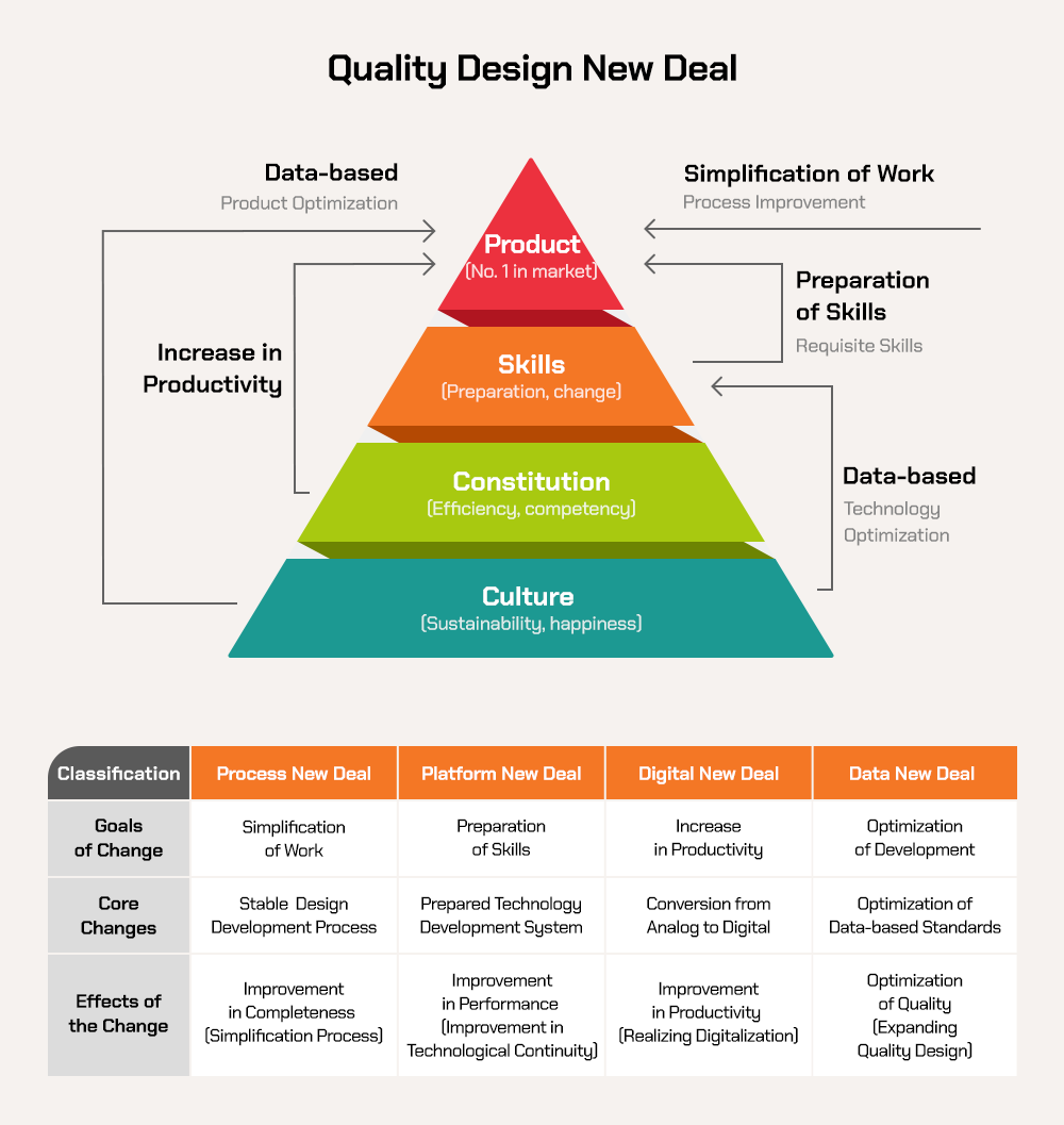
▲ Figure 2. SK hynix’s Quality Design New Deal
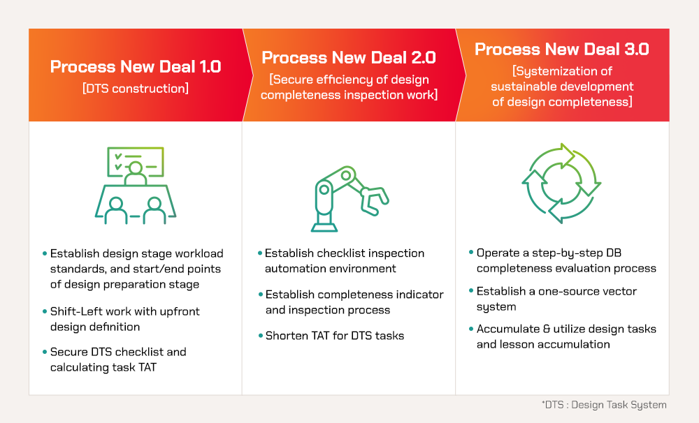
Process New Deal to manage the entire product development process for the world’s best DRAM
DRAM design consists of two stages: design preparation and the design itself. During the design preparation stage, the product target is determined and a competitive product is developed. As part of this stage, the product architecture is reviewed and a pre-checklist inspection is performed to ensure that there are no defects in the design. The design stage ensures the highest level of product characteristics through efficient design based on the items reviewed during the design preparation stage. To accomplish this, it is important to clearly define and execute in detail step-by-step tasks and task-specific checklists during the entire design process.
In the Process New Deal, all matters relevant to the characteristics of the product are described in detail, and the start and end points of the design preparation stage are clearly defined. For successful product development, SK hynix also established the Stage-Gate Process1), an R&D process that manages the entire product development process from idea to launch, with the objective of improving product quality. To improve the design completeness and maximize efficiency in the design stage, the Process New Deal is carried out in three major stages.
▶ Step 1: Build a Design Task System (DTS) that defines all tasks in the design preparation stage, design stage, and product testing stage; determines priorities; and calculates TAT (Turn Around Time) so that check items during the design stage can be prepared in advance. According to the nature of pre-work and project characteristics, three pre-design models are provided to ensure that the design stage can be stably carried out after the design preparation stage.
▶ Step 2: Secure a solution for check items and check methods defined in Step 1, and improve the TAT. This maximizes system efficiency by enabling a quick check of completeness indicators through check automation and digitization.
▶ Step 3: Build a virtuous cycle system that allows the design task system to be advanced while actively utilizing the established DTS. In each design stage, a certain level of step-by-step completion is secured and work is distributed. The accumulated knowledge is included in the integrated test pattern (One-sourced Vector System) that can be verified, to ensure the design completeness is continuously maintained.
By defining and managing all tasks during the design period, the Process New Deal ensures that the time allocated for design work and verification is used through a clear separation between pre-design work and design work. Further, by establishing standards that allow for prompt and appropriate decisions at each stage, the highest level of design perfection is achieved with the optimal amount of manpower and time spent.
▲ Figure 3. Process New Deal
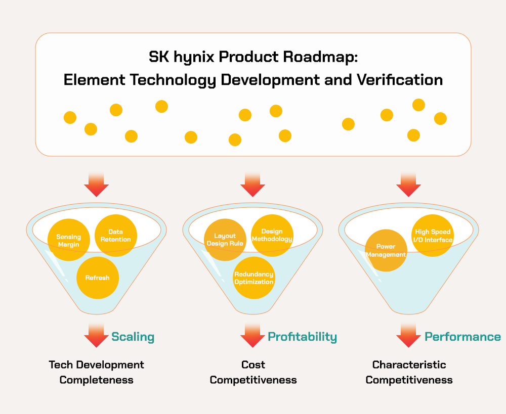
Platform New Deal to build a framework for technologies and work methods required for timely product development
The development of DRAM technology has been limited by several factors, including:
1) Selection of element technology is determined by engineers’ competency and judgment due to the absence of a continuous technology system
2) Insufficient prior inspection of required technology and application of unverified technology
As a result of these limiting factors, the development of the world’s best products was until now at risk, thus necessitating the establishment of a systematic technology platform.
The Platform New Deal verifies all the necessary technologies in advance based on the necessary element technology roadmap, develops the complete technology, and then builds the technology framework and system in the form of packing (Bank Packing) required for product development. The goal is to build a platform, or framework (system), of work methods and to enable timely product development, and consists of three detailed platforms:
▶ Scaling Platform: Prepares a set of technologies (Bank Packing) to ensure Sensing Margin/Data Retention characteristics, which are the main factors for the development of DRAM Process Technology.
▶ Profitability Platform: A technology platform that maximizes Bit Growth2) in each generation of Process Technology, and provides the world’s best cost competitiveness by securing Net Die3) competitiveness. Major technologies include improvement of the Layout Design Rule, minimization of circuit area through Innovative Design Methodology, and optimization of redundancies to improve yield.
▶ Performance Platform: Secures technology with characteristics that consume the least amount of power at the highest speeds in connection with the circuit element technology required for SK hynix’s product roadmap. This industry-leading technology is verified in advance by securing the characteristics of high-performance transistors and operating a test vehicle with design technology (Power Management, High-speed I/O interface) added.
As a result of combining the three platforms, utility is maximized, and final product competitiveness can be ensured. The Scaling Platform provides circuit/process technology that enables the development of new process technology, while the Profitability Platform and Performance Platform ensure product competitiveness. By building a roadmap for required element technology for each product, the technology needed for the future is discovered in advance, and this is then pre-verified using a test vehicle. By utilizing these platforms, SK hynix can create a framework for technologies and work methods and can develop competitive products by filling in necessary technologies according to changing goals, thereby providing a continuous environment for technology development as opposed to a one-time response.
▲ Figure 4. Platform New Deal
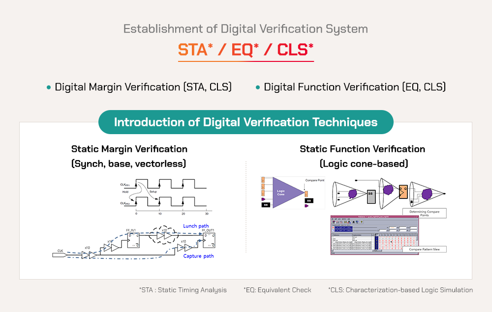
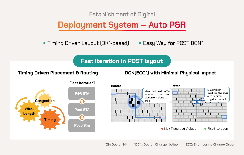
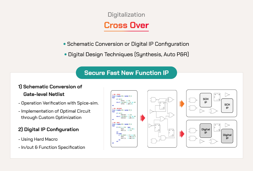
Digital New Deal to encourage changes in the constitution of DRAM design to improve efficiency
In current DRAM designs, a custom DRAM design method is used, giving priority to increasing the net die by minimizing the circuit area. The recent diversification of product lines and the increased capacity and performance of products, however, have led to lower development efficiency. As a result, there is a growing need for standardization, specification, and automation in design digitization.
The purpose of the Digital New Deal is to encourage changes in the constitution of DRAM design through the establishment of digital infrastructure and to establish a system for improving development efficiency using digital design methodologies. To accomplish this, the following three steps are carried out:
▶ Establish digitalization foundation: To develop DRAM STA (Static Timing Analysis) methodology to apply STA, which had been applied to existing logic semiconductor design, to custom DRAM design. By applying STA to DRAM design, high DRAM circuit verification coverage can be achieved within a short period of time without requiring various and complex test patterns. This ensures the completeness of the design stage.
▶ Deploy digitalization: To develop a timing-driven Auto (Auto P&R) method based on the STA environment secured through the previously established digitalization foundation. By developing an method for DRAM, it is possible to increase the productivity of batch design and reduce rigidity, which in turn increases the overall efficiency of development.
▶ Design digitalization: If the meaning of ‘establishing a digitization foundation’ and ‘digitization deployment’ is to achieve digitization of design verification and layout, then ‘design digitization’ refers to digitalization of circuit design. In addition, this secures logic foundry design technology for DRAM, a technology also being discussed for the development of next-generation , and expands the digital design area. By conducting such verification, arrangement, and digitization of circuit design, the constitution of DRAM design can ultimately be changed, and a digital design methodology system specifically designed for DRAM design can be established. Through this, SK hynix can respond to various customer needs and rapidly changing market conditions, and improve the development efficiency of new products.
As part of the Digital New Deal, SK hynix built a digitization infrastructure to change the constitution of DRAM design, and then continued to expand and search for applications that could be incorporated into DRAM design culture. Through standardization, specification, and automation, which are the strengths of digitalization, Sk hynix expects to increase development efficiency in an innovative manner.
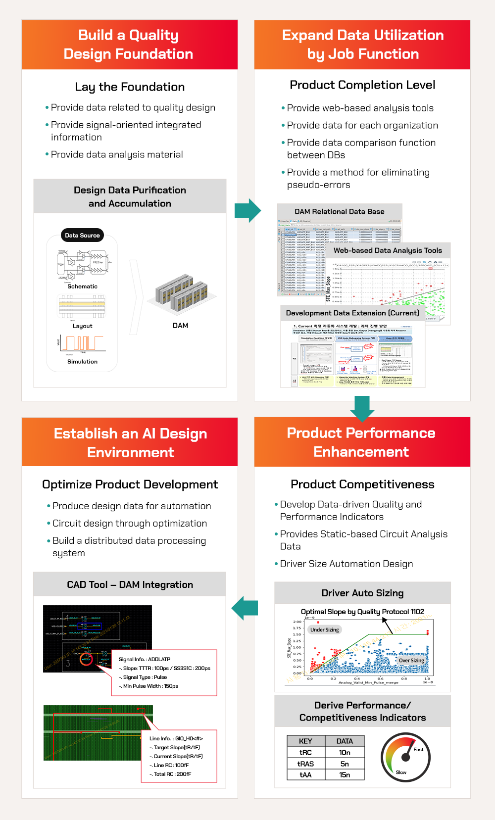
Data New Deal to advance the use of design data and prepare for an AI-based future design environment
In 2021, SK hynix’s DRAM Design group announced its quality design initiative and developed a signal information accumulation information system (DAM) that forms the foundation for quality design. The background of the Data New Deal is to advance the use of design data (circuit, layout, signal information, etc.) accumulated in the DAM. It intends to solve the problems related to DRAM design efficiency and optimization by changing experience-based work to data-based work.
The Data New Deal also aims to ultimately achieve the gradual expansion of the contribution of design optimization using data, and prepare for a future design environment based on artificial intelligence (AI). For this, SK hynix plans to derive new quality protocol and develop an artificial intelligence system for DRAM design (HoVIS, a name that combines hynix and Iron Man’s artificial intelligence system Jarvis).
▶ Derive new quality protocol: Quality protocol can be divided into ‘experience’ and ‘data’. This is to establish a new quality standard for bad cases related to ‘experience’, and to proceed with new quality standardization through the development of n-dimensional multivariate analysis, through which we can derive insights from a large amount of ‘data’.
▶ HoVIS: SK hynix aims to prepare the world’s best DRAM design efficiency and problem-solving capabilities for optimization in terms of future design environments by sequentially developing optimization technologies that will need to be secured for each process-specific task (SPEC, Circuit Design, Pre-, Optimizing, Digital Verification, Unit Verification, Full Chip Verification) expected in the future. As such, the Data New Deal will proceed in the following three stages:
Step 1 is to develop a system that can derive new quality protocol based on data, and to set design completeness as the new quality standard. Step 2 raises the standard of the new quality protocol from design completeness to design performance improvement. And finally, Step 3 raises it from design performance improvement to design optimization to sequentially secure single signal quality, double signal quality, and multiple signal quality.
As such, the new quality protocol standard will be raised from product completeness, to performance, and then to optimization to strengthen the DRAM design. At the same time, if it is used as a standard for an AI-based future design environment connected to HoVIS, we expect the problems of efficiency and optimization can be solved together by transitioning from experience-based work to data-based work.
▲ Figure 6. Data New Deal
Delivering better value to customers
In accordance with the rapidly changing ICT business environment in recent years, there is a growing demand for re-establishing frameworks and standards suitable for this new era. SK hynix’s DRAM Quality Design New Deal policy aims to develop optimized products with the world’s best quality and characteristics. It will also contribute to SK hynix’s ESG management by securing a stable supply of highest quality DRAMs, developing an innovative product development system that is demanded by the global ICT ecosystem, and providing better value to customers. As a first mover in the industry, SK hynix will continue to set new milestones with the frameworks and standards that it creates.
1)Stage-Gate Process: The R&D process that manages the entire product development process. A stage represents when R&D activities are carried out, while a gate evaluates R&D activities at each stage and makes decisions such as whether to continue or stop.
2)Bit Growth: A term used to describe the overall growth rate of memory semiconductors, which is calculated by converting the memory capacity into 1-bit units. A concept introduced to prevent distortion of the growth rate that may occur when calculated based on the number of shipments.
3)Net Die: Number of total dies actually created in wafers.