

A wafer goes through three changes until it becomes a semiconductor chip. The process for the first change is slicing a lump-formed ingot to make a wafer, and the process for the second change is engraving a transistor on the front of the wafer through the front-end process. Finally, in the packaging process, the wafer is divided into individual semiconductor chips, making it a complete semiconductor chip. In the package manufacturing process, which is a back-end process, dicing is performed to divide the wafer into individual chips in a hexahedral shape. Such individualization of a wafer to multiple chips is called “Singulation”, and a process of sawing a wafer plate into a single cuboid is called “die sawing”. Due to the recent increase in the degree of integration of semiconductors, the thickness of wafers is becoming thinner, making the singulation process increasingly difficult.
1. Development of Wafer Dicing

Figure 1. Change of the dicing method for separating into individual chips (singulation)
The front-end process and back-end process develop by influencing each other in various ways. The development of the back-end process is a factor that determines the structure or location of a die (a chip separated in a hexahedral form) on a wafer, or the structure or location of a pad (electrical connection path) on a die in the front-end process. Conversely, the development of the front-end process changes the procedure and method of back grinding or die sawing the wafer in the back-end process. As a result, the appearance of the package which becomes smaller has a great influence on the back-end process. Depending on the changes in the appearance of the package, the number of times for dicing and the procedure and the type of dicing are determined accordingly. ▶ Refer to “Light, Thin, Short and Small”, The Development of Semiconductor Packages Now we will have a look at the five-step dicing method according to the development of chip singulation.
2. Scribe Dicing

Figure 2. Scribe dicing method in the early period: Physical separation (breaking)
after scribing @ wafers with a diameter of 6 inches or less
In the early days, only “breaking”, a method of applying an external force, was performed as a method of separating a die, which is a hexahedral semiconductor chip, with a transistor scribed from a wafer; however, this method caused damages such as chipping (chipped edges) or cracks to a die separated from a wafer. In addition, another problem was that burrs (stumps generated after cutting) of the metal layer were not sufficiently removed, making the cut surface rough.
To prevent these problems, a scribing method where the wafer surface is bladed to a depth of about half before breaking is applied. Scribing means making a groove in advance by sawing (half cutting) the front of a wafer by using a blade wheel. This method of scribing between dies and breaking them into individual chips was mainly used in wafers under 6 inches in the early days.
3. Blade Dicing (or Blade Sawing)

Figure 3-1. Blade dicing (or blade sawing) method @ General conventional method
Scribe dicing has since evolved into a blade dicing (or sawing) method which uses a blade two or three times in a row. This method remedies the disadvantage of chipping, which the edges are broken due to external damage, when breaking after scribing and protects the die during singulation. This can also be referred to as step dicing. Instead of breaking after the first breaking, it performs blading again as the second step.
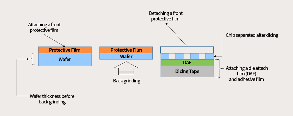
Figure 3-2. Attachment and detachment of film during blade dicing (sawing)
To protect a wafer or a die from external damage during blading, an adhesive tape is attached to the wafer in advance, for safer singulation. Contrary to back grinding where the tape is attached to the front side of the wafer, dicing tape is attached to the back side of the wafer. ▶ Refer to < Back Grinding Determines the Thickness of a Wafer Back> This tape on the back side removes the tape by itself during the process of die bonding, where the separated chip is mounted to the PCB or lead frame. As the friction is high during blading, deionized (DI) water should be continuously sprayed from all directions. In addition, diamond grains are firmly attached to the blade wheel so that it can dig solid silicon better. At this time, the kerf (blade thickness), which is the width of the groove created, must be even, without going beyond the width of the scribe line.
The advantage of blade sawing is that it can cut a large number of wafers in a short time with the conventional method which has been used the most and for the longest until recently; however, if the feeding speed for digging the wafer is increased too much, the possibility of chipping is higher. For this reason, the number of rotations of the blade wheel should be adjusted to around 30,000 times per minute. As this suggests, semiconductor process technology is often established through accumulating know-how obtained through trials and errors for a long time (The next session about die bonding will cover the die attach film (DAF) associated with dicing).
4. Dicing Before Grinding (DBG): Dicing Order Change Method

Figure 4. Existing blading dicing method and dicing before grinding (DBG) method
As the diameter of wafers increased to 12 inches and the thickness became very small, chipping or cracking, which did not cause a big problem even after blade dicing on 8-inch wafers, started to become an issue. In response to this, to drastically reduce the physical damage applied to wafers, a process of dicing before grinding (DBG) was introduced to replace the standard process of conventional dicing. In this method, blading, which was performed in blade dicing, is not performed for two or three consecutive times. Instead, after the primary blading, grinding is performed continuously until the chips are separated while adjusting the thickness of a wafer by back grinding. This method is a more advanced one than the previous blading dicing method. As it has the effect of reducing the damage during the second blading, this method is common in wafer-level packaging.
5. Laser Dicing
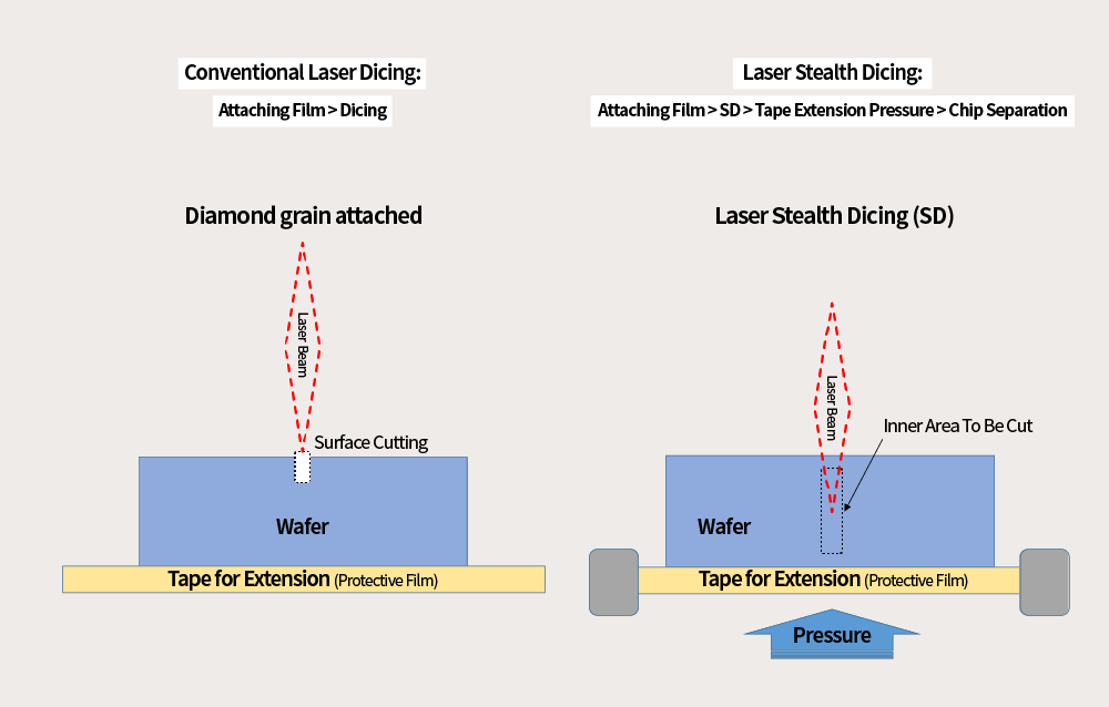
FFigure 5. Comparison of conventional laser dicing (grooving) method and laser stealth dicing (SD) method
For dicing which is applied to processes including wafer level chip scale package (WLCSP) process, there exists a method using a laser. When using this method, the chip quality is excellent with the small amount of chipping and cracking; however, as the productivity is relatively low when the wafer thickness is 100 μm or more, this method is more widely used for thinner wafers. Laser dicing is performed by digging out silicon by applying a laser with high energy to the scribe line of the wafer. In the conventional laser method where the damage created by heat or physical contact with a laser is applied to the wafer surface, grooves are generated and the cut silicon debris adheres to the front surface. For this reason, the wafer surface should be coated in advance to prevent this. The conventional laser method is conceptually similar to blade dicing in the sense of directly cutting the wafer surface.
Laser stealth dicing (SD) is a method which cuts the inner part of a wafer with laser energy first and then applies external pressure to the tape attached to the outside to break the skin and separate the chips. When pressure is applied to the tape attached to the back side, the wafer is instantly bent upwards by the extended tape and the chips are singulated individually. When using this method, there is no debris generated when dicing the surface directly with a laser, and the kerf, the width of the cut line, is also narrowed, so that many chips can be placed on the wafer. In addition, the number of chipping and cracking, which determines the overall dicing quality, is also small. For these reasons, this method is expected to become a popular technology in the near future.
6. Plasma Dicing
Plasma dicing is a dicing method that has been evolving recently. It uses plasma etching in the fabrication (fab) process. This method has less environmental impacts as it uses a semi-gastric material rather than a liquid. Also, as it is applied to the entire wafer all at once, the speed of singulation per chip is relatively fast. In this method, it can be cumbersome in the procedure as a chemical reaction gas is used as raw material and a complicated etching process is required; however, unlike blade dicing or laser dicing which accompanies great and small external damage, there is no external damage in this method, which acts as a great advantage. This reduces the defect rate as well, leading to an increase in the number of chips.
In recent times, the thickness of wafers has been decreasing to 30 μm and copper (Cu) or materials with a small relative dielectric constant (low-k materials) are being used. Accordingly, the plasma dicing method is expected to be more preferred to prevent the occurrence of burrs after processing. Since the technology for plasma dicing is also developing further, it is evolving in a way that allows the use of the etching process without using an etching mask.
As the thickness of wafers has become very thin, from 100 μm to 50 μm, and then to 30 μm, the dicing method for separating it into individual chips is also changing from breaking, blading, and laser to plasma. With the sophistication of the dicing method, the production cost of dicing itself increases, but dicing defects frequently found in semiconductor chips such as chipping and cracking have significantly decreased. Also, due to the increased number of chips on the same wafer, the production cost per chip decreases. The increase in the number of chips per unit area is related to the narrowing of the dicing street width (kerf width) within the scribe line, along with the evolution of the dicing method. The number of chips on a wafer where plasma dicing is applied can be increased by nearly 20% compared to blade dicing. Because of this economic effect, the plasma method is preferred. In addition to wafer processing technology, various dicing process methods such as DBG are emerging according to the external changes of wafers and chips, and the package method.

ByJong-moon Jin
Teacher at Chungbuk Semiconductor High School


