Semiconductor substrates refer to wafers in a broad sense. On the wafer surface, we directly stack transistors, which are basic elements of semiconductor circuits, or build a new layer to use as a substrate to form components on top of it. In particular, transistors for special purposes such as those for communication, military, and optical elements, or high-performance and high-quality transistors require an epitaxial wafer. In this chapter, we will take a look at the formation process, use, and characteristics of the ultra-hyper pure layer, the so-called “epitaxial layer”, which is a layer newly formed on a wafer made of ultra-pure silicon.
1. Epitaxial Layer, an “Ultra-hyper Pure” Layer over an Ultra-pure Wafer
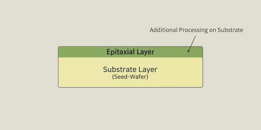
▲ Figure 1. Initial seed-wafer and epitaxial layer with additional processing
Wafers are manufactured in the wafer manufacturing process, separately from the semiconductor manufacturing process. When transforming molten silicon into an ingot of high purity close to 100% and cutting it into a plate shape, wafers are completed. For wafers, various materials are used, ranging from silicon, which is most frequently used for integrated circuits, and germanium, to gallium arsenide for high-speed analog use.
Most wafer manufacturing processes have a similar flow in general, though some of them are slightly different in terms of process conditions and methods. Silicon wafers are categorized into three: ultra-pure wafers, impurity (P/N type) wafers, and epitaxial wafers with additional processes. Among these, silicon wafers doped in p-type are most commonly used. This is because CMOSFETs can be simply manufactured as soon as N-Well (semiconductor manufacturing process) is formed on a P-type substrate. Epitaxial wafers, or epi wafers, are completed after going through an additional process called the epitaxial process where ultrapure wafers are used as a seed (medium).
2. Prerequisite of Epitaxial Layer: Crystalline Structure
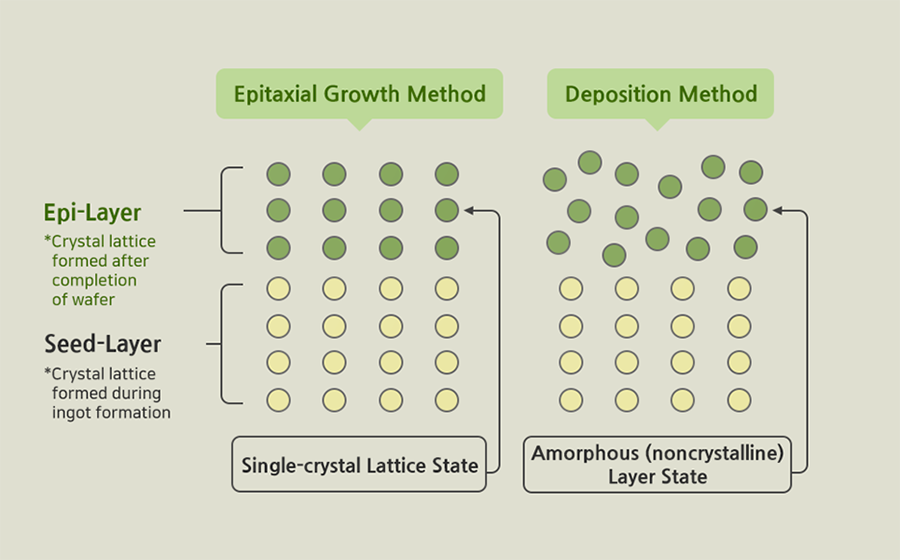
▲ Figure 2. Epitaxial layer vs Amorphous layer
The prefix “epi-” means ‘upon’ or ‘on top of’ and epitaxial refers to a layer made in the upper direction. Epitaxial growth can be also called epitaxy or epi in short. This means stacking additional new layer with the growth into a single crystal, which is a solid where all crystals of one type are regularly generated along a certain crystal axis, while a seed wafer is placed underneath and the lattice direction is maintained.
In the transistor structure, substrates that serve as the paths for the flow of drain currents, should have a crystalline structure; however, since most of the deposition methods used in the early semiconductor manufacturing process have noncrystalline (amorphous) layers, special conditions and methods should be adopted to make epitaxial layers grow to avoid an amorphous state.
To be used as a seed-layer, the lattice composition should be crystalline, while inheriting the crystal lattice structure of the lower layer for upward growth. Therefore, it is necessary to have a layer where the alignment of the lattice is regular and the lattice constants are consistent or almost similar. Here, a new layer or substrate formed by a special method on the seed-layer is called an epitaxial layer, and a wafer on which an epitaxial layer is formed is called an epitaxial wafer.
3. Conditions for Electron Flow within Crystal Lattice
One of the functions of semiconductor components is to move electrons, detect and judge the movement, and use the judgment result as On/Off information. The reason for adding another process (ultra-hyper pure) on the seed-wafer is to make a layer with no defect to facilitate electrons’ move in the zero-defect field.
To increase mobility of electrons in a certain direction, the crystal lattice should be regularly arranged. It is better if the distance between atoms is constant. In other words, polycrystalline or noncrystalline (amorphous) lattice arrangement weakens electron mobility and causes electron traps, making it difficult to predict and manage the gate voltage and drain current.
4. Crystal Lattice Constant
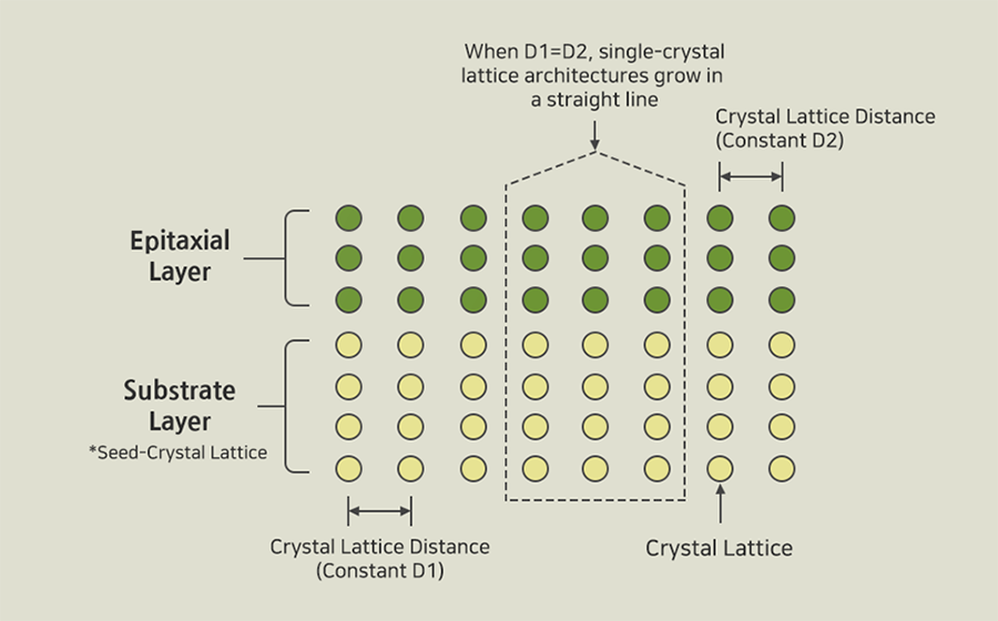
▲ Figure 4. Lattice constants of the epitaxial layer and single-crystal structure
A lattice constant refers to the distance of the bonds (covalent bonds) between silicon atoms. Any entry of a third element in the middle leads to a change in the quantity of electric charge, resulting in a change in the distance between atoms (lattice constant). It is important to maintain the lattice constant little changed if possible. If the inconsistent lattice constant results in a change in thermal expansion coefficient of the upper and lower layers, it could cause a wafer warpage. Also, when stacking SiO2 or HfO2 as a gate oxide layer, stacking an oxide layer over an ultra-hyper pure layer with a crystal lattice constant unified through epitaxial growth, rather than over a partly impure silicon substrate, can minimize electron traps between interfaces and mismatches (weakened adhesion, etc.) between interfaces.
Despite its excellent quality, epitaxial layers are used only in special cases due to the complicated process and high cost. In particular, as the epitaxial process requires growth in a single crystal, the speed of processing is slow.
5. Lattice Match & Mismatch
When a seed-layer and an epitaxial layer have the same distance in the crystal structure, we call it homoepitaxy, and when it is not, we call it heteroepitaxy. In the case of heteroepitaxy, when the crystal lattice distance of the epitaxial layer is larger, compressive stress is applied to match it to the seed-layer distance. On the contrary, when the crystal lattice distance is smaller than that of the lower layer, tensile stress is applied to increase the distance.
The form where atoms are combined is called a crystal structure or a lattice. If there is a mismatch in the distances between atoms within the crystal structure, unwanted defects such as voids and hillocks are caused, resulting in quality issues. Any dislocation or electron trap can be avoided if a new epitaxial substrate is grown on the substrate. On top of this, if the epitaxial layer is doped while being formed, a layer can be created in a desired type of impurity, allowing it to be used as a substrate for forming semiconductor components.

By Jong-moon Jin
Teacher at Chungbuk Semiconductor High School