

Artificial intelligence (AI), which is regarded as the ‘the most significant paradigm shift in history,’ is becoming the center of our lives in remarkable speed. From autonomous vehicles, AI assistants to neuromorphic semiconductor that mimics the human brain, artificial intelligence has already exceeded human intelligence and learning speed, and is now quickly being applied across various areas by affecting many aspects of our lives. What are the key applications of AI technology and how is it realized?
(Check here to discover more insights from SNU professor Deog-Kyoon Jeong about AI semiconductor!)
Cloud Computing vs. Edge Computing

Figure 1. Cloud Computing vs. Edge Computing
One AI application, which is an antipode to cloud services, is edge computing1. Applications that require processing massive amounts of input data such as videos or image data must process data using edge computing or transfer the data to a cloud service through wired or wireless communication preferably by reducing the amount of data. Accelerators specifically designed for edge computing for this purpose take up a huge part of AI chip design. AI chips used in autonomous driving are a good example. These chips perform image classification and object detection by processing images that contain massive amounts of data using CNN2 and a series of neural operations.
AI and the Issue of Privacy


Another area of AI application is conversational services like Amazon’s Alexa or SK Telecom’s NUGU. However, such services cannot be used widely if privacy is not protected. Conversational AI services, where conversations at home are continuously eavesdropped by a microphone, cannot be developed beyond a simple recreational service by nature, and therefore, many efforts are being made to resolve these privacy issues.
The latest research trend in solving the privacy issue is homomorphic encryption3 . Homomorphic encryption does not transmit users’ voice or other sensitive information such as medical data as is. It is a form of encryption that allows computations of multiplication and addition on encrypted data in the form of ciphertext, which only the user can decrypt, on a cloud service without first decrypting it. The outcome or results are sent to the user again in an encrypted form and only the user can decrypt to see the results. Therefore, no one including the server can see the original data other than the individual user. Homomorphic service requires an immense amount of computation up to several thousand or tens of thousand times more compared to the general plaintext DNN4service. The key area for research in the future will be around reducing the service time by dramatically enhancing computation performance through specially designed homomorphic accelerators5.
AI Chip and Memory
In a large-scale DNN, the number of weights is too high to contain all of them in a processor. As a result, it has to make a read access whenever it requires a weight stored in an external large capacity DRAM and bring it to the processor. If a weight is used only once and cannot be reused after accessing it, the data that was pulled with considerable amount of energy and time consumption will be wasted. This is an extremely inefficient method as it consumes additional time and energy compared to storing and utilizing all weights in the processor. Therefore, processing an intense amount of data using enormous number of weights in large-scale DNN requires a parallel connection and/or a batch operation that uses the same weights over several times. In other words, there is a need to perform computations by connecting several processors with DRAMs in parallel to disperse and store weight or intermediate data in several DRAMs to reuse them. High speed connection among processors is essential in this structure, which is more efficient compared to having all processors access through one route. And only this structure can deliver the maximum performance.
Interconnection of AI Chips

Figure 3. Interconnection Network of AI Chips
The performance bottleneck that occurs when connecting numerous processors depends on the provided bandwidth, latency as well as the form of interconnection. These elements define the size and performance of the DNN. In other words, if one were to deliver ‘N-times’ higher performance by connecting ‘N’ number of accelerators in parallel, bottleneck occurs in the latency and bandwidth provided by the interconnections and will not be able to deliver the performance as one desires.
Therefore, the interconnection structure between a processor and another is crucial in efficiently providing the scalability of performance. In the case of NVIDIA A100 GPU, NVLink 3.0 plays that role. There are 12 NVLink channels in this GPU and each provides 50 GBps in bandwidth. Connecting 4 GPUs together can be done by direct connections using 4 channels each in the form of a clique. But to connect 16 GPUs, an NVSwitch, which is an external chip dedicated just for interconnection, is required. In the case of Google TPU v2, it is designed to enable a connection of a 2D torus structure using Inter-Core Interconnect (ICI) with an aggregate bandwidth of 496 GBps.
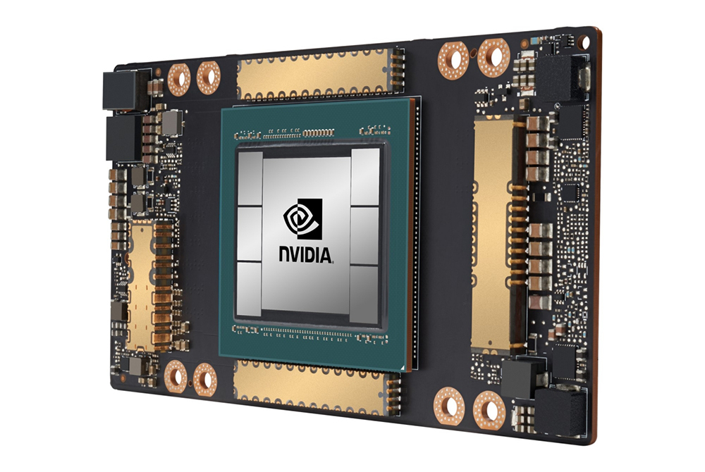
Figure 4. NVIDIA’s GPU Accelerator A100 using 6 HBMs
(Source: The Verge)
The way in which processors are interconnected has a huge impact on the whole system. For example, if they are interconnected in a mesh or torus structure, the structure is easy to compose as the physical connection between chips is simple. But latency increases proportionally to the distance as it requires hopping over several processors to interconnect between nodes that are far away. The most extreme method would be in the form of a clique that interconnects all processors one to one, but this would lead to a significant increase in the number of chip pins by N!, causing PCB congestion beyond allowable so that in actual design, connecting up to only four processors would be the limit.
Most generally, using a crossbar switch like a NVSwitch is another attractive option, but this method also converges all connections on the switch. Therefore, the more the number of processors you want to interconnect, the more difficult the PCB layout becomes as transmission lines concentrate around the switch. The best method is structuring the whole network in a binary tree, connecting processors at the bottom end, and allocating the most bandwidth to the top of the binary tree. Therefore, creating a binary fat tree will be the most ideal and will be able to deliver maximum performance with scalability.
Neuromorphic AI Chip

Figure 5. Cloud Server Processor vs. Neuromorphic AI Processor
Data representation and processing method of processors for cloud servers that serve as DNN accelerators take the form of digital, since the computational structure is fundamentally simulation of NN through software on top of hardware. Recently, there is an increase in research on neuromorphic AI chip which, unlike the previous simulation method, directly mimics the neural network of a living organism and its signals and maps to an analog electronic circuit and performs in the same manner. This method takes the form of being analog in the representation of original data in actual applications. This means that one signal is represented in one node, and the interconnection is by hardwire and not defined by the software, while the weights are stored in an analog form.

Figure 6. Previous semiconductor vs. Neuromorphic semiconductor
The advantage of such structure is that it has maximum parallelism to perform with minimum energy. And neuromorphic chips can secure great advantage in certain applications. Because the structure is fixed, it lacks programmability, but it can offer a great advantage in certain edge computing applications of a small scale. In fact, neuromorphic processor has significance in applications such as processing AI signals of sensors used in IoT by delivering high energy efficiency or image classification that requires processing large amounts of video data using CNN of a fixed weight. However, because the weight is fixed, it will be difficult to use in areas of applications that require continued learning. Also, it is difficult to leverage parallelism that interconnects several chips in parallel due to a structural limitation when it comes to large-scale computations, making its actual area of application restricted to edge computing. It is also possible to realize the neuromorphic structure in a digital form, and IBM’s TrueNorth is an example. It is known, however, that the scalability is limited, making it difficult to find wide practical applications.
Current Status of AI Chip Development
To create a smart digital assistant that can converse with humans, Meta (formerly known as Facebook), which needs to process massive amounts of user data, is designing an AI chip specialized to have basic knowledge about the world. The company is also internally developing AI chips that will perform moderation to decide whether to post real-time videos that are uploaded to Facebook.
Amazon, a technology company that mainly focuses on e-commerce and cloud computing, has already developed its own AI accelerator called AWS Inferentiato power its digital assistant Alexa and uses it to recognize audio signals. Cloud service provider AWS has developed an infrastructure that uses the Inferentia chip and provides services for cloud service users that can accelerate deep learning workloads like Google’s TPU.
Microsoft, on the other hand, uses field programmable gate array (FPGA) in its data centers and has introduced a method of securing the best performance by reconfiguring precision and DNN structure according to application algorithms in order to create AI chips optimized not only in current applications, but also in future applications. This method, however, creates a lot of overhead to refigure the structure and logic circuit even if it has identified an optimal structure. As a result, it is unclear that it will have actual benefit because it is inevitably disadvantaged in terms of energy and performance compared to ASIC chips specifically designed for certain purposes.
A number of fabless startups are competing against NVIDIA by developing general-purpose programmable accelerators that are not specialized to certain areas of application. Many companies, including Cerebras Systems, Graphcore, and Groq, are joining the fierce competition. In Korea, SK Telecom, in collaboration with SK hynix, has developed SAPEON and will soon be used as the AI chip in data centers. And Furiosa AI is preparing to commercialize its silicon chip, Warboy, as well.

Figure 7. SAPEON X220
(Source: SK Telecom Press Release)
The Importance of the Compiler
The performance of such AI hardware depends greatly on how optimized its software is. Operating thousands or tens of thousands of computational circuits at the same time through systolic array and gathering the outcome efficiently require highly advanced coordination. Setting up the order of the input data to feed numerous computational circuits in the AI chip and make them to work continuously in a lockstep and then transmitting the output to the next stage can only be done through a specialized library. This means that developing an efficient library and the compiler to use them is as important as designing the hardware.
NVIDIA GPU started as a graphics engine. But NVIDIA provided a development environment, CUDA, , to enable users to write programs easily and enabled them to run efficiently on the GPU, which made it popularly and commonly used across the AI community. Google also provides its own development environment, TensorFlow, to help develop software using TPUs. As a result, it supports users to utilize TPU easily. More and more diverse development environments must be provided in the future, which will increase the applicability of AI chips.
AI Chip and its Energy Consumption
TThe direction of AI services in the future must absolutely focus on enhancing the quality of service and reducing the required energy consumption. Therefore, it is expected that efforts will focus around reducing power consumption of AI chips and accelerating the development of energy-saving DNN structure. In fact, it is known that it takes 10^19 floating-point arithmetic in the training of ImageNet to reduce error rate to less than 5%. This is the equivalent to the amount of energy consumed by New York City citizens for a month. In the example of AlphaGo that was used in the game of Go against 9-Dan professional player Lee Sedol in 2016, a total of 1,202 CPUs and 176 GPUs were used in the inference to play Go and estimated 1 MW in power consumption, which is tremendous compared with the human brain using only 20 W.
AlphaGo Zero, which was developed later, became a system of a performance that exceeds AlphaGo merely after 72 hours of training using self-play reinforcement learning with only 4 TPUs. This case proves that there is potential in reducing energy consumption using a new neural network structure and a learning method. And we must continue to pursue research and development on energy-saving DNN structures.
The Future of the AI Semiconductor Market
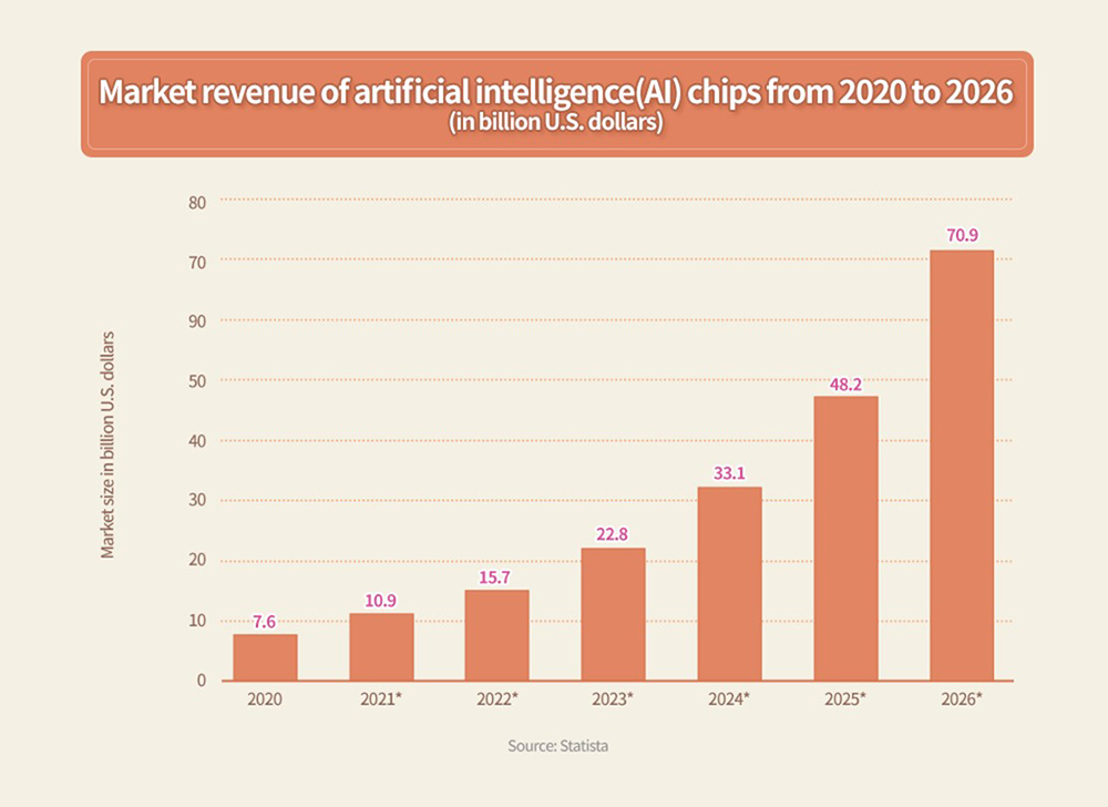
Figure 8. AI Chip Market Outlook
(Source: Statista)
The successful accomplishments made in the field of AI will expand the scope of application, triggering stunning market growth as well. For example, SK hynix recently developed a next-generation intelligence semiconductor memory, or processing-in-memory (PIM)6, to resolve the bottleneck issue in data access in AI and big data processing. SK hynix unveiled the ‘GDDR6-AiM (Accelerator in Memory)’ sample as the first product to apply the PIM, and announced the achievement of its PIM development at the International Solid-State Circuits Conference, ISSCC 20227, an international conference of the highest authority in the field of semiconductor, held in San Francisco in the end of February this year.

Figure 9. GDDR6-AiM developed by SK hynix
Application systems will further drive a wider AI market and continuously create new areas, enabling differentiated service quality backed by the quality of inference based on a structure of neural network. AI semiconductors, which are the backbone of the AI system, will be differentiated based on how fast and accurately they can conduct inference and training tasks using low energy. Latest research findings show that energy efficiency per se is extremely poor. Therefore, there is an increasing need for research on new neural network structures with a focus not only on function, but also on energy efficiency. And in terms of hardware, the core element that defines energy efficiency lies around improving memory access methods. As such, Processing-In-Memory (PIM), which processes within a memory and not by accessing memory separately, and neuromorphic computing that mimics the neural network by storing synapse weights in analog memory will become important fields of research.
1Edge computing is a distributed computing paradigm that brings computation and data storage closer to the sources of data.
2Convolutional neural network (CNN) is a type of artificial neural network used in image recognition and processing that is specifically designed to process pixel data.
3Homomorphic encryption is a form of encryption that permits users to perform computations on its encrypted data without first decrypting it.
4A deep neural network (DNN) is an artificial neural network with multiple layers between the input and output layers.
5An accelerator is a special-purpose hardware made using processing and computation chips.
6Processing in memory (PIM, sometimes called processor in memory) is the next-generation technology that provides a solution for data congestion issues for AI and big data by adding computational functions to semiconductor memory. The product based on such technology is sometimes known as a PIM chip.
7The International Solid-State Circuits Conference was held virtually from Feb. 20 to Feb. 28 this year with a theme of “Intelligent Silicon for a Sustainable World.

ByDeog-kyoon Jeong, Ph.D.
Professor
Electrical & Computer Engineering
Seoul National University(SNU) College of Engineering


