Today, artificial intelligence (AI) technology is being used across such a wide spectrum of applications that it has some people even predicting that AI could start to exceed human intelligence in the next 20 years and begin threatening the existence of mankind.
While we are unaware, AI technology began showing remarkable results across several different areas, from license plate recognition, voice recognition, and autonomous driving to translations, natural language interactions, and games. It also excelled in creative applications of “human-only” actions that had been deemed impossible to replicate through technology, such as composing music and creating paintings.
The ability of technology to replicate the problem-solving capabilities of humans stems from a computation method of Neural Networks1 that’s completely different from how earlier computers would have performed.
Currently, many researchers are attempting to solve problems that were difficult to solve with existing methods by using such artificial neural networks. And starting with the 21st century, it became a new way of problem-solving that gained the most attention along with Quantum computing2. Conventional computers perform algorithms that were designed with the von Neumann architecture, which is based on a mathematical model grounded in Boolean algebra3. In the 20th century, it was the best tool for solving problems. However, we have entered the 21st century of AI, which delivers a completely different capability.

Figure 1. Timeline of neural network in early stage
While the neural network technology has only recently been used in applications, it has a long history. In the early stages of AI research, there were various AI technologies that emulated the decision-making abilities of humans, such as the expert system, which organized and formalized knowledge to suggest solutions, as well as script-based conversational agents that enabled interactions with the computer. Neural network was also a method of problem solving at the time but was seen as being too primitive and having too many limitations to be commercialized.

Figure 2. Neuron in our brain
The neural network is fundamentally based on the mechanism of the brain. After it was neuroanatomically proven that neural networks consist of both neurons and synapses between neurons, Warren McCulloch and Walter Pitts developed a mathematical model of a neural network in 1943. Known as a perceptron model, it proved its ability to perform various logical operations until 1969, when prominent mathematicians Marvin Minsky and Seymour Papert pointed out that the perceptron model could only solve linear equations and was incapable of learning even a simple XOR function4, which prompted many to shift their attention elsewhere. Also, the method of learning and determining synapse weight, which was key to neural network calculation, was challenging. That made it even harder to put the method into practical use.

Figure 3. Neural network
In 2010, Professor Geoffrey Hinton at the University of Toronto proposed a simple, yet groundbreaking, method of adopting an activation function called Rectified Linear Unit (ReLU). It would enable the computer to learn, without losing accuracy, synapse weight by penetrating the multi-layers, essentially performing back propagation of knowledge from output to input. It was a turning point in the history of neural network research. And in 2012, Professor Hinton’s research group published AlexNet, an architecture that applies the learning method of deep neural network in image classification, the most challenging problem in the field of computer vision. This led to significantly overcoming the existing technology’s limitations.
During this process, the Convolutional Neural Net (CNN) model, which emulates the retinal structure of processing images captured in the retina of cats, was introduced. Eventually, a performance level that was comparable to the way a person would analyze an image. Deep neural network refers to a neural network that has a deep vertical structure of more than 10 hidden layers, compared to the average neural network, which has 4 to 5 layers. The computational workload required in such a process is tremendous, which makes it difficult to use with an existing computer because it would require too much time. But tech company NVIDIA leveraged the Graphics Processing Unit (GPU) computing power developed for a graphics card with massively parallel processing function to build Deep Neural Networks (DNN) for problems that could not be solved with conventional methods and enabled training of the synapse weight in a short period of time.
This led to great progress. DNN was applied to many other applications. And many researchers competed to study the new DNN structure. As a result, the problem-solving ability of AI, represented by DNN, developed rapidly, and penetrated many application areas, becoming a panacea for solving difficult problems.
Artificial Intelligence (AI) Semiconductor
It was the development of hardware, centered around the GPU, that enabled the development of DNN over its theoretical basis to application. Without the massive calculation capabilities of GPU, the development of artificial intelligence would have been very slow.
But to ultimately create an AI that transcends the human ability, it will require higher performance computing power than what’s available today. The key lies within the next-generation AI semiconductor that outperforms the current GPU.
It is known that there are approximately 85 billion human neurons and that there are about 1,000 – 10,000 times more synapses that connect the neurons to each other than there are actual neurons. To emulate the human brain, a synapse weight of about 85 trillion to 850 trillion would be required, as would a large storage device to store those values.
This scale of calculation structure is beyond the abilities of current semiconductor manufacturing, but it is expected that a specifically designed artificial intelligence semiconductor (AI chip) could handle it.
According to forecasters, a semiconductor chip that comprises such an AI system will see a rapid performance improvement and exponential marketability, along with the expansion of applications. It is expected to grow to about KRW 52 trillion (approximately USD 44 billion) by 2024 and to KRW 140 trillion (approximately USD 120 billion) by 2030.
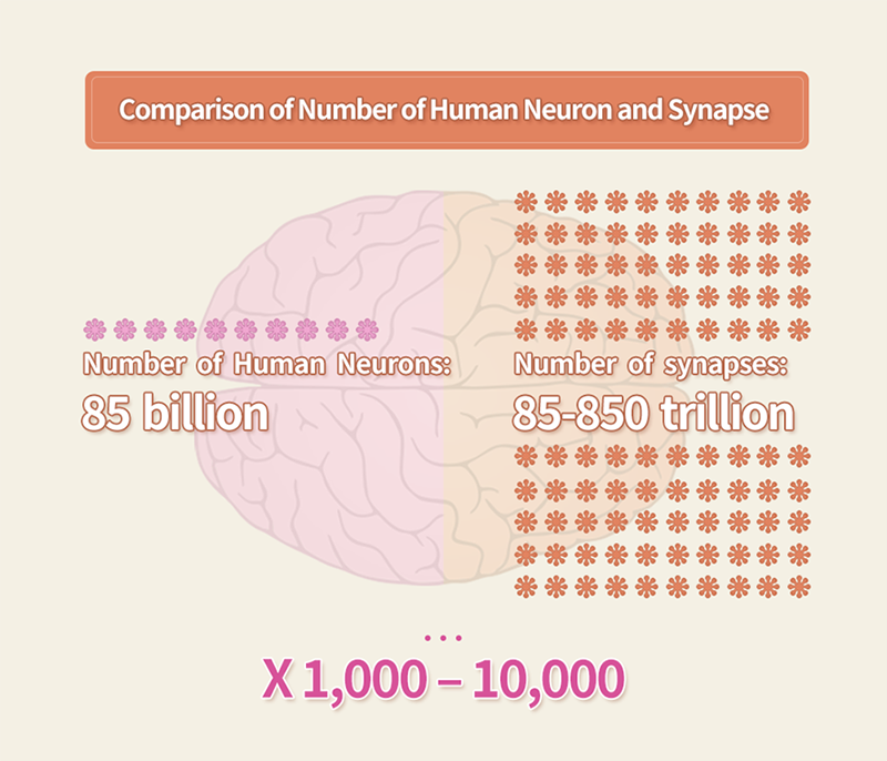
Figure 4. Comparison of number of human neuron and synapse
AI semiconductor can be largely classified into chips for cloud service and chips for edge computing, depending on the area of application. The required specifications differ greatly, while both markets are expected to be similar in size. The AI chip can also be categorized into two specialized areas that are based on functionality. Those for inference and for data training, which generally includes the function of the former.
Inference refers to unilateral calculation that delivers the output to the input based on what was already trained. It is mostly comprised of matrix vector multiplication of 8-bit or less precision. By contrast, chips for training, which require high precision of 16 to 32 bits, perform training on various data batches as a way to quickly train a massive amount of data. This requires matrix-matrix operations, which leads to a lot more calculations and consumes much more energy than simple inference. However, once training is performed and synapse weight is defined, the work shifts to a large amount of low-power AI chips that are specialized solely for inference.
Dedicated AI Semiconductor
As the strongest player in the cloud service market, Google leads its competitors in its focus on operating AI services more efficiently. The company is especially aware that it takes a dedicated and specialized processor that can handle a deep learning workload computation that’s used in AI in a faster and more efficient manner. Realistically, using tech company NVIDIA’s GPU is the most reasonable option, but GPUs are fundamentally for image rendering and performing ray tracing calculations. As such, a programmable SIMD (single-instruction, multiple data) processor structure is adopted. While it’s optimized for processing high-speed game graphics and can be applied to various applications because it is programmable, it’s inefficient for DNN and lacks the efficiency to perform deep learning or machine learning workloads for cutting-edge AI applications.
In addition, the GPU supports graphics data, which is different from what is required for AI. And the method of calculation is different, meaning that while it delivers useful function, it is unfavorable when it comes to energy efficiency. To overcome these limitations and develop Google’s own processor specialized for AI service, the company formed a processor architecture team in 2013 and began to develop a Tensor Processing Unit (TPU). By 2015, the Google-developed semiconductor chip was being applied to its cloud service. Specific functions and composition of the chip was unknown until it was disclosed in 2017. The TPU has an enormous matrix that holds the synapse weight to efficiently perform DNN’s inference function along with the function to multiply the vectors of each layer’s input. Its performance was also significantly improved by adopting a systolic structure to enable necessary calculations both in parallel and in pipeline without wasting time.
Here, tensor refers to multi-dimensional matrix of more than two dimensions. The first chip developed by Google was for inference of two dimensions without a training capability, while the second TPU chip can calculate multi-dimensional functions, as well as a training capability.
Google TPU
Google’s first-generation TPU5 Application-Specific Integrated Circuit (ASIC) was built on a 28nm process. This TPU was used in the game of Go, which was considered a game difficult to play against human players with only the conventional computer, and in designing the AI-powered Go program AlphaGo. The TPU beat Lee Sedol, a professional Go player of 9 dan rank, by 4 to 1 at the Google DeepMind Challenge Match in March 2016. The win demonstrated that the ability of AI to exceed a human’s ability.
The TPU chip is fundamentally an accelerator for inference and is not appropriate for training purposes, or in other words, learning the weight, which is another aspect of DNN processing. Since then, Google announced 2nd generation TPU v2 in 2017, v3 in 2018, and v4 in 2020, which not only can accelerate inference, but also training. And it adopted next generation 2.5D (2.5 dimensional) High Bandwidth Memory (HBM) over the previous DDR memory for the external memory.
HBM, which emerged as a new type of memory, is significantly better than DDR DRAMs that were mostly used in previous servers. It has 4 or 8 vertically stacked DRAM chips with more storage capacity than before. It can also deliver outstanding performance by allocating more than 2,000 connecting lines and connecting them via Si interposer, rather than the printed circuit board (PCB) that was previously mostly used, to significantly improve input/output performance. As a result, HBM has become an essential memory in building high-performing systems.

Figure 4. SK hynix HBM3
Today, SK hynix manufactures HBM2E and has successfully developed next generation standard HBM3, maintaining a leading position in the market. Data on system management is necessary to find the most efficient structure in developing dedicated chips for AI, and because Google runs a large cloud service center, it is easy to secure the required data. It can gather various data on identifying the actual workload mix and understanding the bottleneck in service efficiency to efficiently manage its AI service. As such, it can have a system in place to continuously develop AI accelerators that are optimized based on the data. As a result, it is expected that Google will be able to continuously respond to changes by developing new chips across various areas of application.
NVIDIA’s GPU
Meanwhile, NVIDIA continues to develop new models to use GPU6 as programmable processors not only for graphics, but also to efficiently use for AI, and they are designed with the flexibility to respond to various applications However, lack the performance and energy efficiency of Google’s TPUs, which are optimized for a few specific applications. It is important for NVIDIA to collect operation data such as workload mix across various applications from cloud service operators like Google, Facebook, Amazon, and Microsoft in order to continue to develop competitive GPUs. And it must continue to focus on chip development to remain competitive in the continuously changing field of application.
Custom AI Semiconductor
Today, designing and manufacturing processors are no longer exclusive to specialized companies like Intel, AMD, or Samsung Electronics. Anyone can design efficiently using highly advanced Design Automation Tools and produce custom processors with optimized functions for their own applications through foundries that provide cutting-edge processing. In fact, Apple uses chips of its own design in the application processors (AP) of iPhones and has even designed its own CPU for PC devices, significantly improving the performance and energy efficiency of Mac, which used to use Intel chips.
The highest performing model of Apple’s M1 chip is the M1 Max, which reaches up to 3.2GHz. It has 57 billion transistors and 10 cores, and its performance and energy efficiency are exceedingly better compared to the most recent 11th Gen i9 processor from Intel. On the other hand, the difficulty in adopting an optimized processor structure due to command-line compatibility issue with previous processors is a weakness of Intel’s processors and the trend of developing optimized, unique processors for specialized applications will continue in the future.
For cloud service operators, there will be a huge differentiation in the quality of service depending on whether they use a general processor or a specialized processor for certain DNN application. However, designing and developing such chips will take a huge amount of capital and resources, which means that only a few large cloud service operators can consider developing AI chips in a way where the benefits exceed the costs. Along with this trend, many independent companies specializing in semiconductor design are developing general-use AI chips for cloud services that exceed the performance of NVIDIA GPU. But that requires obtaining huge amounts of data on workload mix collected in the process of cloud service operators managing their services to develop competitive and efficient AI chips. Therefore, AI chip-specializing fabless design companies must pursue joint development with cloud service providers.
1Neural Network, usually called Artificial neural networks, are computing systems inspired by the biological neural networks that constitute animal brains.
2Quantum computing is a type of computation that harnesses the collective properties of quantum states, such as superposition, interference, and entanglement, to perform calculations.
3Boolean algebra is the branch of algebra in which the values of the variables are the truth values true and false, usually denoted 1 and 0, respectively.
4‘Exclusive or’ or ‘exclusive disjunction’ is a logical operation that is true if and only if its arguments differ (one is true, the other is false).
5Tensor Processing Unit
6Graphic Process Unit

ByDeog-kyoon Jeong, Ph.D.
Professor
Electrical & Computer Engineering
Seoul National University(SNU) College of Engineering