Considerable research has been conducted on developing emerging memories to create a high-performance and cost-effective bridge between CPU/DRAM and SSD storage from the perspective of the memory hierarchy*. In recent years, Compute Express Link (CXL)* has emerged and memory tiers have been suggested for optimizing performance and capacity at each workload. Due to its capability for both persistency and capacity expansion, 3D XPoint (3DXP)* has attracted attention as a memory solution to fill the gap between DRAM and storage.
*Memory hierarchy: Memory can be divided into a hierarchy based on speed as well as use. A typical memory structure includes cloud, flash, DRAM, cache and register memories.
*Compute Express Link (CXL): PCIe-based next-generation interconnect protocol on which high-performance computing systems are based.
*3D XPoint (3DXP): Developed by Intel and Micron, 3DXP is a non-volatile phase change technology that serves as both memory and storage. Cell arrays consist of simple stackable crossbar structures for multiple layers.
This article will focus on research into developing a four-deck 3DXP solution which was presented at the 2023 Very Large-Scale Integration (VLSI) Symposium, one of the world’s top three semiconductor conferences. It also considers the scaling limitations of 3DXP and the potential for selector-only memory (SOM) to be the future of storage class memory (SCM).
Advancing 3DXP Through Novel Integration Schemes
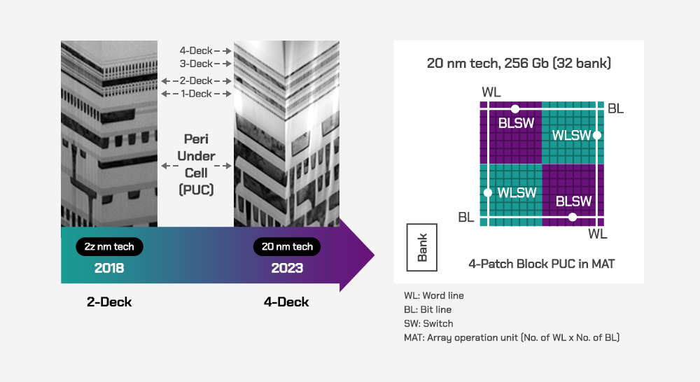
▲ Figure 1. (Left) Cross section transmission electron microscopy (TEM) of two-deck and four-deck cell arrays with a copper multi-layer and peri under cell (right) Floorplan of a 20 nm four-deck chip with a capacity of 256 Gb
SK hynix has made significant progress in its development of 3DXP memory solutions over the past few years. At the 2018 International Electron Devices Meeting (IEDM), SK hynix shared the results of its two-deck 64 Mb test chip operation with 2z* nanometer (nm) technology, and then successfully demonstrated a 128 Gb chip in 2019. More recently, the company demonstrated progress on a four-deck 256 Gb chip with 20 nm technology at the 2023 VLSI.
*2z: The third generation of 20 nm process technology in which “z” refers to the lower third number range of the 20 nm class, which covers 20 nm-29 nm. The letters “x”, “y” and “z” are used to refer to the upper, middle, and lower thirds, respectively, of the relevant process technology class such as 10 nm, 20 nm etc.
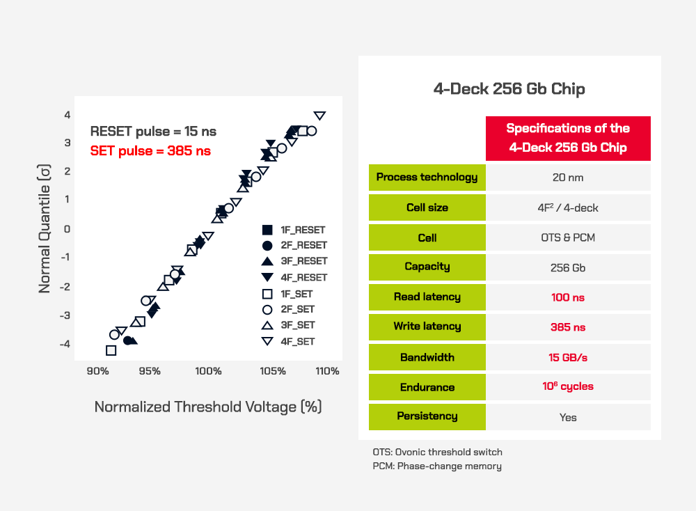
▲ Figure 2. (Left) Voltage distribution of each deck after set and reset operations (right) Basic die information, including structure and operation properties, of the four-deck chip
To create this latest solution, SK hynix developed novel integration schemes including new self-align etching, cleaning, chemical mechanical polishing (CMP), and interlayer dielectric (ILD) deposition. A low-resistance conductor material was also developed for the interconnection scheme to ensure a sufficient flow of write current while minimizing spike current. In addition, a large read window margin* and a tight voltage distribution of the 1 Gb array for each deck were achieved by carefully controlling the 20 nm pillar patterning process, material design, and appropriate write/read operation.
*Read window margin (RWM): The threshold voltage (Vt) interval (ΔVt) at distribution tails. When using a chalcogenide material such as PCM, it has a Vt distribution similar to DRAM or NAND. The Vt interval between the Vt distribution of 0 and 1 is regarded as the sensing margin, or the read window margin.
Overcoming Limitations of 3DXP With SOM
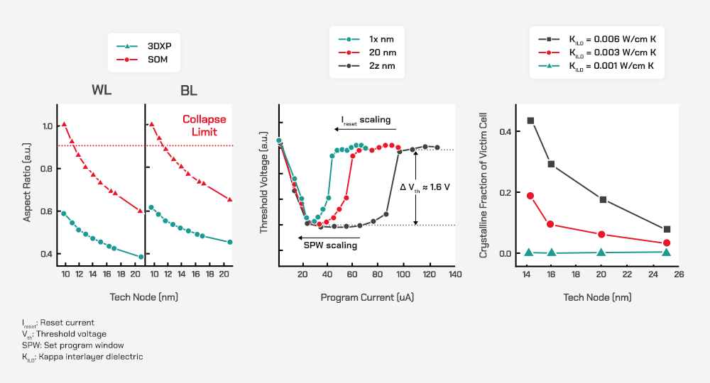
▲ Figure 3. Scaling challenges of 3DXP presented in three graphs: (left) Aspect ratio (center) Set program margin (right) Thermal disturbance
Although the researchers successfully demonstrated a four-deck 256 Gb device, they discovered issues when assessing the scalability of 3DXP beyond 20 nm technology. First, the structure of 3DXP, which consists of phase-change memory (PCM)* and an ovonic threshold switch (OTS)*, will have a much higher aspect ratio* as the technology is scaled down and this will lead to complex progress integration. Second, 3DXP will have a smaller write program margin between set and reset operations as the technology node shrinks. Third, the scaling limit by thermal disturbance is expected to occur at technology nodes beyond 1y nm without the elusive thermal conductivity of inter-layer dielectric.
*Phase-change memory (PCM): A technology which enables nonvolatile electrical data storage at the nanometer scale. A PCM device consists of a small active volume of phase-change material placed between two electrodes. A common PCM material is germanium-antimony-tellurium (GeSbTe).
*Ovonic threshold switch (OTS): A two-terminal symmetrical voltage sensitive switching device which, after being brought from the highly resistive state to the conducting state, returns to the highly resistive state when the current falls below a holding current value.
*Aspect ratio (AR): The ratio of height to width. A high aspect ratio means that the structure is narrow but tall.
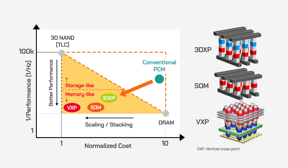
▲ Figure 4. Memory requirement relationship between performance, which indicates bandwidth, and cost
As a result of these limitations, SK hynix is preparing SOM as an alternative solution for the next generation of storage class memory. SOM is composed of only two electrodes and a single dual-functional material which can operate as both the memory and selector. Compared to 3DXP, SOM offers lower write latency and cell power consumption as it eliminates 3DXP’s long crystallization time for the set operation and high reset current. Therefore, SOM is set to be a leading solution for next-generation applications with scaling longevity beyond 1z nm technology.
For more information regarding RTC’s research, please visit the center’s research website (https://research.skhynix.com). The RTC operates the site to share insights on its ongoing research of future technologies and to actively communicate with various global research organizations.