Applying Light to Semiconductors: Introducing to CIS Key Process Technologies
Cameras are one of the media which record objects embodied by light, allowing people to express various emotions, identity, and philosophy either objectively or subjectively. In particular, we are in a so-called “digital nomad era” where people carry digital devices and live without being restricted from time and space. In this era, digital cameras equipped with image sensors are more widely used than film cameras. It is also the era of smartphones, which are equipped with digital camera functionality. In digital cameras or smartphone cameras that record our daily life and memories, the role of image sensors is like films in film cameras. Image sensors play a key role in converting the information of the subject received through the lens into an electrical image signal.
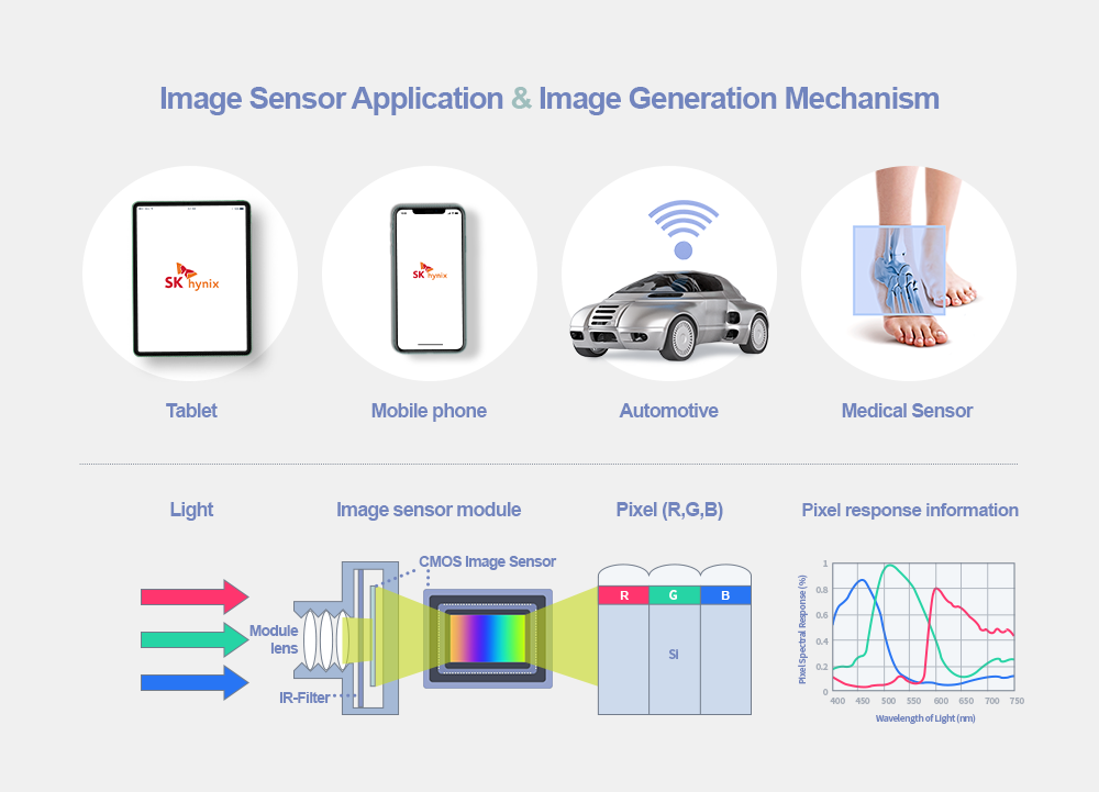
▲ Figure 1. Image sensor applications & Image generation mechanism
Image sensors can be largely divided into CCD image sensors and CMOS image sensors based on their applications and manufacturing processes. In particular, CMOS image sensors (CIS) are going beyond digital cameras and are actively applied to various new market fields, such as smartphones, tablets, CCTVs, black boxes for cars, autonomous vehicle sensors, virtual reality (VR), medical equipment, and drones. Through this, sales of this semiconductor product line are showing rapid growth*.
The operation process of a CMOS-based image sensor is as follows: When the light energy in the visible light wavelength range (400 to 700nm) is condensed on the photodiode (PD) of the silicon substrate, the silicon surface receives the light energy to form an electron-hole pair. The electron generated in this process is converted into voltage through floating diffusion (FD) and then converted into digital data through an analog to digital converter (ADC). To make such a CIS product making the series of these processes possible, key manufacturing process technologies unique to CIS, which are different from the ones for semiconductor memory, are required. These process technologies can be classified into five categories.
1. Deep PD Formation Process Technology
Consumers’ desire for clearer image quality led to competition to increase the pixel density and resolution in mobile CIS, accelerating the development of CIS process technology. The pixel size should be more reduced to increase the number of pixels in the same chip size. Also, forming deep PD is a key technology to avoid deterioration in image quality. To secure sufficient full well capacity (FWC) in small pixels, patterning and implementing technologies with higher difficulty level compared to the ones for semiconductor memory are required. Especially, it is essential to secure a high aspect ratio (>15:1) implant MASK process technology that can block high-energy ion implantation; in fact, the aspect ratio tends to be gradually increasing in the industry these days*.
![]()
▲ Figure 2. Schematic diagram of photo diode structure change along with reduction in pixel size
2. Pixel to Pixel Isolation Process Technology
The technology to isolate pixels from one another is very important to make a high-definition CIS. A less developed isolation technology can cause various image defects such as color mixing and color spreading. Each chipmaker has different isolation technology, and the difference will be an important criterion for image quality in the CIS market where higher pixel density and higher resolution are becoming common standards. Various issues can occur during the isolation process. For this reason, huge efforts are being made to select better equipment and develop new recipes to improve yield and product quality.
3. Color Filter Array (CFA) Process Technology
Color filter array (CFA) is a process unique to CIS that is not seen in the semiconductor memory process. The CFA process is generally composed of a color filter (CF) that filters the incident light into red, green, and blue for each wavelength range, and a microlens (ML) to increase efficiency in condensing. To create excellent image quality, it is important to develop and evaluate R/G/B color materials and develop technologies to optimize process conditions such as shape and thickness. Recently, a series of high-quality and high-functional CIS products are being released, thanks to the development of various application technologies such as Bayer and Quad being combined with the basic form of CFA.
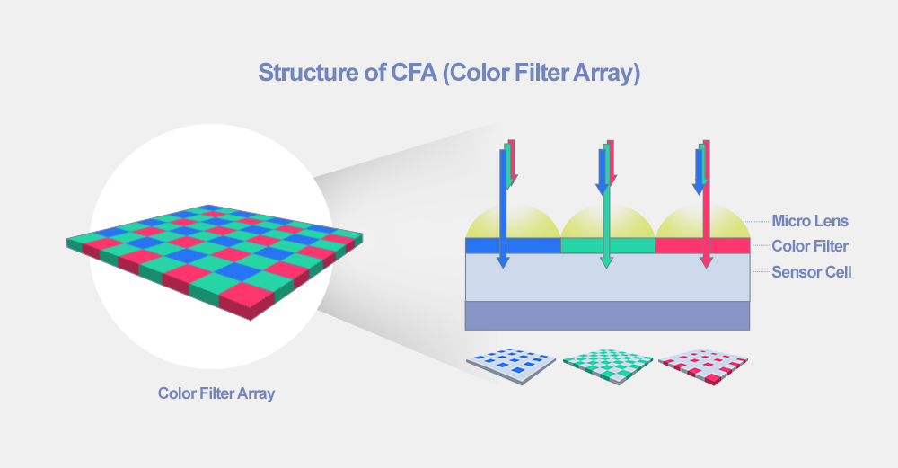
▲ Figure 3. Structure of CFA (Color Filter Array)
4. Wafer Stacking Process Technology
Wafer stacking refers to attaching two wafers together. This is an essential technology for making high-pixel and high-definition CIS products*. For high-pixel CIS products, pixel arrays and logic circuits are formed on individual wafers separately. These wafers are attached together in the middle of the process, which is called “wafer bonding”. Separation of the pixel arrays and logic circuits would increase manufacturing cost, but more chips can be produced in the same amount of wafer area, and it also helps improve product properties. As a result, it is a technology adopted by most CIS chipmakers these days. Wafer stacking technology is continuously developing in various forms. Recently, the wafer stacking technology has been applied to the semiconductor memory segment as well, contributing to the improvement of the product properties.
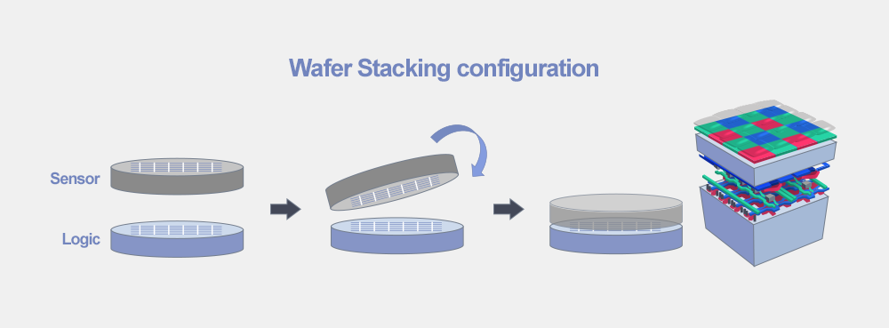
▲ Figure 4. Wafer Stacking configuration
5. Control Technology to Improve CIS Product Yield and Quality
One of the most fundamental requirements in the CIS product development and mass production process is to control metallic contamination. Since CIS products are sensitive to contamination several times more than memory products and the contamination directly affects product yield and quality, various contamination control technologies are required. The next important factor is the plasma damage* * control. Since the deterioration of image properties such as hot pixels occurs due to the damage caused during the process, it is necessary to manage key processes accurately.
This article covered the main characteristics of the key CIS process technologies. It is no exaggeration to say that the completeness of CIS products is determined by not only the process technology, but also how organically pixel devices, analog and digital design, and image signal processing (ISP) technology are complementing each other and being optimized. Based on the existing semiconductor memory process technologies, SK hynix has secured the core process technologies which are unique to CIS products, including the ones listed above. Through this, the Company is proactively responding to the market demand, with the in-time development of high-pixel and high-definition products. In the future, based on its process technologies, devices, design, and ISP technology, the CIS business of SK hynix is expected to expand its base to various application product lines in different fields, such as medical and security, as well as mobile CIS products. Ultimately, it is expected that this will contribute to the creation of both economic and social values that SK Group pursues.
*Yole Development, “Status of the CMOS image sensors industry 2012”, https://www.slideshare.net/Yole_Developpement/yole-cmos imagesensorsoctober2012reportsample
*SONY.net, “Perspectives from the creators of the image sensor ‘microcosm’” https://www.sony.net/SonyInfo/technology/stories/IMX586/
*Cheng-Ta Ko, et al., “Wafer-to-wafer hybrid bonding technology for 3D IC” 3RD Electronics System Integration Technology Conference ESTC, Berlin, 2010, pp. 1-5, doi: 10.1109/ESTC.2010.5642848.
*Koji Eriguchi, “Defect generation in electronic devices under plasma exposure: Plasma-induced damage” Jpn. J. Appl. Phys. 56 (2017)
*K. Eriguchi., “Application of Molecular Dynamics Simulations to Plasma Etch Damage in Advanced Metal-Oxide-Semiconductor Field-Effect Transistors”, Molecular Dynamics− Studies of Synthetic and Biological Macromolecules, 221-244 (2012)

In-Chul Jeong
CIS Process Team Leader at SK hynix Inc.