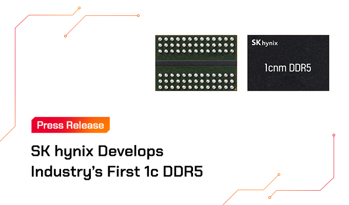
Semiconductor scaling is one of the most important topics of the industry. As most of electronic devices and memory cells represented by DRAMs are micro-miniaturized, there is a need for high-integration technology that allows even small-sized devices to store astronomical amounts of data that can be processed all at once. Now considered as the core of semiconductor scaling, the Extreme Ultra Violet (EUV) process is a next-generation lithography technology. Now, SK hynix is actualizing its dream of mass-production of the next-generation DRAMs by constructing its new cutting-edge memory semiconductor plant ‘M16’. Located in Icheon, South Korea, this new plant is expected to have separate spaces dedicated to EUV equipment.
“Moore’s Law is dead” – Semiconductor scaling hits a dead end
In semiconductor scaling, existing ‘multi-patterning’ is now unavailable courtesy of argon fluoride (ArF) lithography technology exposing its limitations on the newly adopted 10nm scale. In the semiconductor industry, ‘Moore’s Law’ stated that chip density doubles every 24 months. It held strong for a while but now faces its end due to the higher difficulty of photolithography processing.
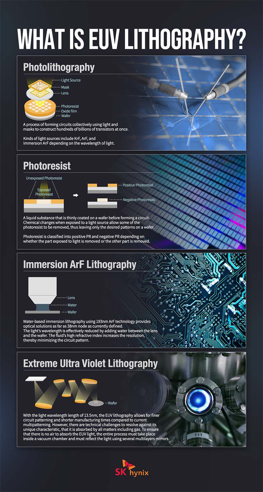
Semiconductor production requires a photolithography process in which a thin yet powerful laser beam prints meticulous micro-circuit patterns onto a wafer, similar to how a photo is printed–which is why it is called ‘photo.’ ‘Photolithography’ is a technology which transfers and copies the shadows created by lighting a ‘mask’, or an original glass plate with metal patterns of the desired circuit design. This is one of the most crucial steps of the entire manufacturing process as these patterns are imprinted onto the wafer, with the accuracy of the circuit’s design ultimately determining its competitiveness in the market.
‘Scaling’ represents the industry’s supreme task, shortening the gate length within a transistor on a semiconductor circuit. The gate acts like a bridge between a source and a drain, controlling the flow of the current. Thus, as the gate length decreases, the amount of electron movement from a source to a drain increases accordingly, which in turn accelerates the circuit’s operating speed.
Semiconductor lithography equipment has seen many advances over the years, adopting a large lens with high numeral aperture (NA) or using short wavelength light as the light source. However, as gate length decreases below 30nm, the patterning ability of existing liquid immersion ArF lithography equipment reaches its limit. Whilst a multi-patterning method was applied for DRAMs of up to 18nm, this created additional processing stages and prompted productivity loss and increased material costs, which all resulted in escalating production costs. As the number of processing steps reached nearly 500 to 600, the only solution was painting minute circuit patterns with a ‘thinner brush,’ via the application of even shorter wavelength light.
Pioneering EUV technology could lead the way
Accordingly, the semiconductor industry has been preparing for new semiconductor lithography under the name EUV to enable 10nm-class scale processes. Dutch company ASML has a monopoly on EUV equipment and each unit costs between about USD 81 million and USD 122 million. By utilizing the light of a 13.5nm wavelength, much shorter than existing ArF wavelength of 193nm, EUV allows much finer semiconductor circuit patterns without multi-patterning. Through this, the number of processing steps is reduced and thus manufacturing time shorter than current multi-patterning, such as Quadruple Patterning Technique (QPT), giving EUV pioneering status as the only breakthrough to date.
However, applying EUV to chips like DRAMs is a challenging process requiring the most advanced technology around. For this reason, the industry is keeping a close eye on the yield of the DRAMs that are mass-produced by EUV for the first time. Regarding DRAMs, it is expected that EUV will be partially used in 2020 in manufacturing chips of 1ynm or smaller.
Resolving technological challenges in EUV processing is the key
Resolving the technological challenges of EUV processing is vital for the future of the industry. EUV has a unique characteristic of being absorbed by nearly every matter, even gases. Therefore, it is necessary to develop new technologies first over the whole range of lithography process, including a new mask, photoresist, and optical systems. It is crucial to manufacture masks with no defects and to ensure developing new mask test equipment as well.
Increasing the number of wafers produced per hour is another important challenge. In 2018, ASML achieved a wafer per hour (WPH) of more than 125 and is aiming to break the 155 mark in 2020. In terms of light source output, it is known that DRAM manufacturers’ tests results showed up to 250W. Semiconductor manufacturers which started developing EUV processes with equipment bought from ASML are now at developing and testing the overall equipment. The industry is conducting research on high-NA processes of 0.55NA as the next-generation of lithography technology, beyond the 0.33NA currently being developed.
“For the successful mass-production of EUV lithography technology, securing technologies to manufacture EUV masks that assure zero defects, as well as hardware within lithography equipment, light sources and pellicle, is essential,” said an official from the semiconductor industry. “Research on a variety of technologies that test for defects within EUV masks is currently ongoing. For improved resolution, utilizing the light source of shorter wavelengths and securing higher NA are crucial.”

By Eunji Jang
Journalist of News1, one of the biggest newswires in South Korea