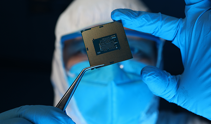
It’s very challenging to further miniaturize components that are already only a few nanometers wide.
The history of electronics is a study in the progression and evolution of miniaturization, as electrical systems matured and migrated to become what we now consider electronics. The reason older tech is huge is that it was full of individual components that were literally wired together. All of the electronics processes that we do today, with digitally driven solid-state devices, had to be done in a brute-force analog manner.
In the case of the transistors that make up our modern microcontrollers and processors, the antique analog versions were called vacuum tubes [1], variations on light bulb technology originally discovered in 1880 by Thomas Edison. Exited metal plates between filament grids in the vacuum-sealed glass bulbs regulated the passage of current but were very power inefficient (because they were modified light bulbs) and very fragile (also because they were modified light bulbs).
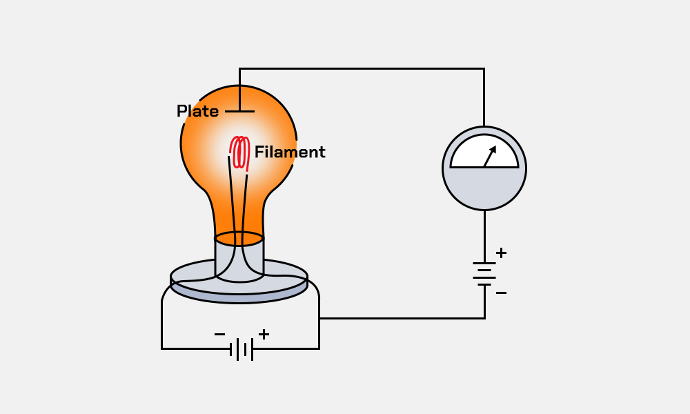
▲ Figure 1. Circuit diagram of the Edison discovery.
These issues of power and size in electronics were such a fundamental aspect of early electronics that it shaped both popular and professional history. The first computers and their rows upon rows of vacuum-tube-filled racks engulfed a large room and gave off so much heat that the first computer bug reported was an actual insect attracted to the tubes [2]. Even in science fiction, an art designed to inspire futuristic thought, most authors predicted powerful computers—none predicted small pocket-sized smart devices.
Kilby, Noyce, and the Birth of the Chip
The discovery of the semiconductor and the creation of solid-state transistors in the 1960’s began the evolutionary process in electronics [3], laying the foundation for the world we have today. Instead of using a brute-force approach of wires and grids in a vacuum tube, a semiconductor device works by controlling the passage of electrons through a solid monocrystalline piece of semiconducting material. (There is an entirely different revolution going on in semiconductor materials, which we’ll touch on later.)
These semiconductor devices, even in their first iterations, were significantly smaller, lighter, better performing, cooler operating, and much more efficient than their glass-based forefathers. The breakthrough in semiconductors enabled the creation of the integrated circuit (IC), although there were several important technology hurdles that had to be overcome. These included the actual forming of devices in the crystal, the need to electrically isolate components, and the creation of electrical connections within the IC.
The birth of the IC is a story in parallel development. Jack Kilby, a radio engineer and World War II veteran, made the first hybrid IC in May 1958 from germanium [4], followed closely in January of 1959 by Robert Noyce, who unveiled his design of a planar integrated circuit [5]. Since then, semiconductor devices have been continuously miniaturizing.
Later on, in the early 70’s, IC feature device size (the space between the components and connection vias) decreased to 10 μm, and the number of the MOSFETs in a chip exceeded 1,000 [6]. In modern days, chips have gone down to 7nm spacing, with 5nm planned, and work underway for 2nm and less.
I/O, Logic, and Power
There are many aspects that need to be addressed when making electronics smaller in general, including the integration and management of the data input/output (I/O), the logic IC itself, and the power needed to drive it all. The demands of each create a juggling act the electronic designer must perform when creating products.
At the circuit-board level, miniaturization involves high levels of component integration. For example, a product could require an inertial sensor, a compass, temperature and presence sensors, as well as those for images and light. An integrated sensor module groups sensors based on related technologies into a single package, saving significant space.
Meanwhile, package-level miniaturization forces include the shrinking of power electronics due to the advent of new wide-bandgap semiconductors. These new materials, Gallium Nitride (GaN) and Silicon Carbide (SIC) are enabling a 60%+ reduction in the size of power supplies while also increasing performance by up to 300% [7]. They are enabling significant reduction in products simply by making the power electronics smaller.
We must consider the circuit-level miniaturization process as well, which relies on simplifying and/or optimizing the system. This approach leverages advances in device integration and the new power electronics, which enable advanced circuits with smaller passive devices and significantly smaller footprints. It can be leveraged with next-generation user interfaces that eliminate the need for a keypad or other space-hungry input method.
When it comes to logic devices, all issues at the macro-level must also be addressed at the chip level. How many devices can be integrated on a chip? How closely can the components of a chip be put together before they start interfering with one another? How do you get power in the right amount (current) and level (voltage) to the parts of the chip that need it?
Shrinking the Chip
There are several limiting factors when it comes to miniaturization. The first limit is defined by basic physics, in this case the distance of atoms in the material. It’s literally impossible to make the device structures less than the atomic distance, which does define a true lower limit to nano-electronics. This lower limit isn’t the real final barrier to miniaturization, however, as there is a fundamental limit defined by the distance the electrons can tunnel in the material.
The smaller chips get, the harder it is to control aspects like the leakage current between the source and drain of the transistors involved. This is regarded as one of the main limits to miniaturization, because it’s impossible to suppress the diffusion of electrons from the source to the channel at normal temperatures.
Still, the industry will continue to shrink electronic devices of all types because they are critical to so many aspects of our future smart Cloud-enabled Internet of Things (IoT)-oriented society. Both at the macro-level and the micro-level, expect to see higher levels of component integration, both planar and 3D, as well as further advances in materials for both the chips and their interconnects.
In the sense of vertical integration, SK hynix’s 176-layer 512 Gigabit (Gb) Triple-Level Cell (TLC) 4D NAND flash is a good example of the current state of the art [8]. The third generation 4D product that allows the bit productivity to be improved by 35% and the read speed increased by 20% over legacy devices. The data transfer speed also has been improved by 33% to 1.6Gbps without increasing the number of processes.
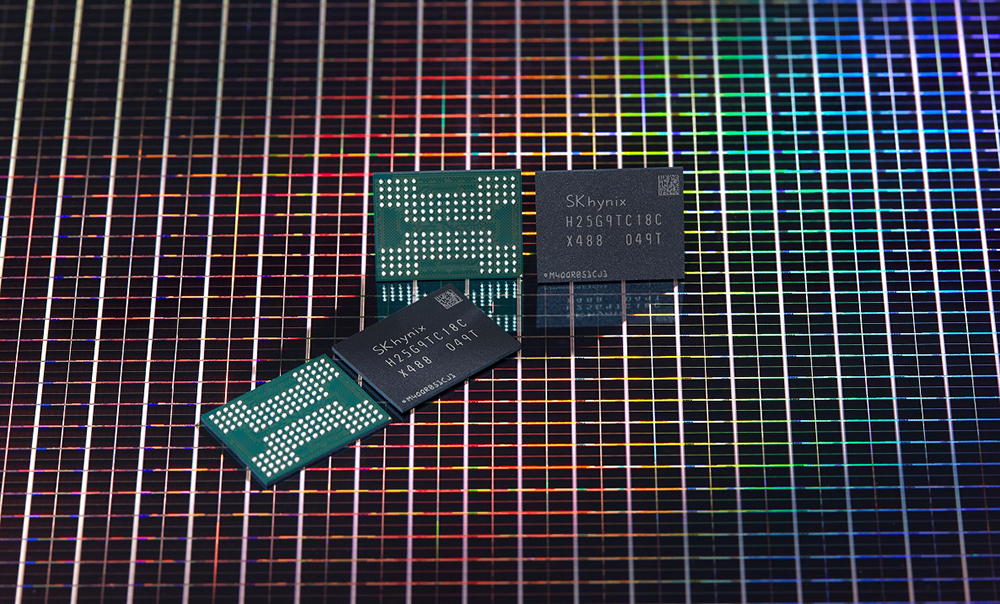
▲ Figure 2. SK hynix’s 176-layer 512 Gb TLC 4D NAND Flash
In regard to material advancements, just as piezoelectric semiconductors like Gallium Nitride have revolutionized the power electronics industry, they offer the promise to do the same for logic chips. One of the major benefits of a piezoelectric semiconductor is its ability to switch at extremely high speeds. Currently advanced GaN power devices can switch up to 40 MHz [9], and if these materials can be adapted to logic circuits, could enable a jump of several orders of magnitude in processor performance at the same feature size.
Another area of approach to miniaturize chips is to improve the way we flash the mask pattern onto the wafer itself. The more we can improve pattern resolution, the closer we can get to the theoretical limits in smaller sizes. The latest lithography methods [10] use short wavelengths in the blue or ultraviolet range.
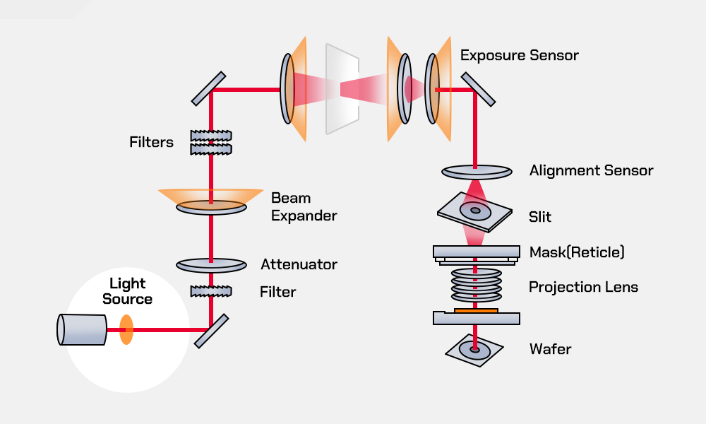
▲ Figure 3. A diagram of EUV equipment
For instance, in the semiconductor memory industry SK hynix recently announced the mass production of its cutting-edge 1anm 8Gb LPDDR4 DRAM by using EUV equipment [11]. As one of the first to successfully implement the technology in mass production, several other major manufacturers are expected to follow in SK hynix’s footsteps as confidence grows in the application of EUV.
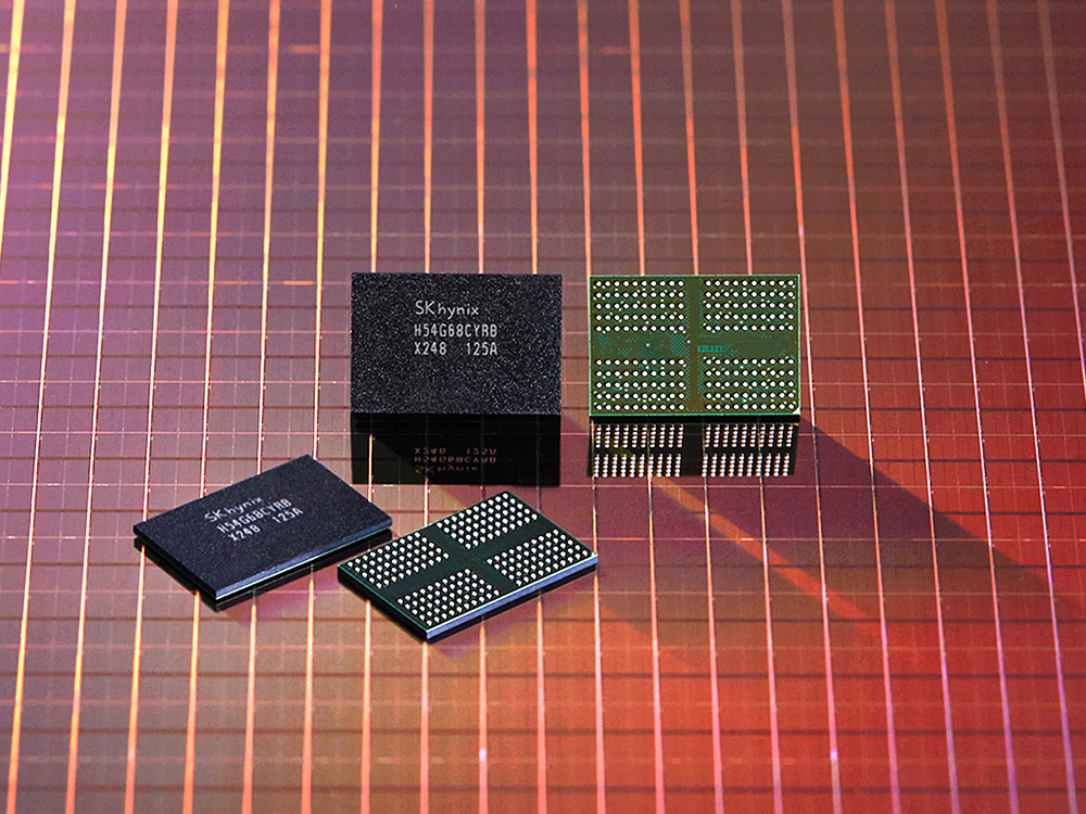
▲ Figure 4. SK hynix’s 1anm 8Gb LPDDR4 DRAM Using EUV Equipment
Integration is key
Another aspect of design where the micro mimics the macro is in the integration of functionality. Just as a product can be made smaller by integrating various devices on the circuit board, the circuit itself can be made smaller by integrating function blocks into the chip.
By providing functions that used to require their own device, highly integrated chips enable a significant reduction in the board space used [12]. Where once even a “simple” smart product needed a microcontroller (MCU), a power management IC (PMIC), an RFIC, and a chip to control the user interface at the least, can now be served by a single-chip solution, requiring only a display, antenna, and a battery (packaging too) to create a basic product.
All of the developments in component integration, next-generation functionalities, and even packaging advances come together to create the micro-product revolution going on as you read this. Another often-overlooked aspect in the effort to shrink a product involves flexible electronics. Making flat, flexible, and efficient electronics opens the door to countless smart products that were impractical due to size or form-factor issues.
The ability to bend, fold, roll, and even stretch will enable electronics to not only expand more deeply into market sectors like medical and sports wearables, advanced portable and small robotics applications, and the Internet of Things, it will also enable those products to be rolled up and/or folded and easily stored between uses. Optimizing a product design by highly integrating its functionality at the chip, board, and product level pays major dividends.
Bulky keyboards and large screens will eventually cease to be a size issue when flexible electronics and non-contact means of data entry are further commercialized. Reducing the impact of the user interface on product design cannot be underestimated, as every external opening is removed not only reduces the form factor demands, but also increases water resistance and product durability. Optimizing a product design by highly integrating its functionality at both the chip and board level pays dividends at each.
Looking Forward
The advanced electronics and the semiconductors behind them are the sophisticated result of decades of research and development, both in functionality and scaling. The demand for smaller and smaller technology will never diminish, as the new functionalities delivered today create new expectations for tomorrow. The semiconductor industry must continue in its efforts to innovate and keep shrinking electronic components to keep pace with the demands of society in the areas of technological advancement, in even the tiniest of ways.
[Reference]
[1] ScienCentral. (n.d.). The Vacuum Tube. ScienCentral and The American Institute of Physics, 1999. https://www.pbs.org/transistor/science/events/vacuumt.html
[2] National Geographic Society. (2014, July 18). World’s First Computer Bug. https://www.nationalgeographic.org/thisday/sep9/worlds-first-computer-bug/
[3] The semiconductor revolution. (n.d.). Encyclopedia Britannica. https://www.britannica.com/technology/electronics/The-semiconductor-revolution
[4] Kilby, J. (n.d.). Jack Kilby Biography. NobelPrize.Org. https://www.nobelprize.org/prizes/physics/2000/kilby/biographical/
[5] Lovos, M. (2018, June 7). Robert N. Noyce Biography. IEEE Computer Society. https://www.computer.org/profiles/robert-noyce
[6] The Electrochemical Society. (2021, April 13). Impact of Micro-/Nano-Electronics, Miniaturization Limit, and Technology Development for the Next 10 Years and after. Newswise. https://www.newswise.com/articles/impact-of-micro-nano-electronics-miniaturization-limit-and-technology-development-for-the-next-10-years-and-after
[7] Navitas. (2021, August 27). SHARGE Upgrade 100W Fast Charging: 60% Smaller than Legacy Silicon. https://navitassemi.com/navitas-and-sharge-upgrade-100w-fast-charging-60-smaller-than-legacy-silicon/
[8] SK hynix Unveils the Industry’s Most Multilayered 176-Layer 4D NAND Flash. (2020, December 24). SK Hynix Newsroom. https://news.skhynix.com/sk-hynix-unveils-the-industrys-highest-layer-176-layer-4d-nand-flash/
[9] Jha, J., Ganguly, S., & Saha, D. (2021, May 12). GaN-based complementary inverter logic gate using InGaN/GaN superlattice capped enhancement-mode field-effect-transistors. IOP Science. https://www.scribbr.com/apa-citation-generator/new/webpage/
[10] Markoff, J. (2015, September 26). Smaller, Faster, Cheaper, Over: The Future of Computer Chips. The New York Times. https://www.nytimes.com/2015/09/27/technology/smaller-faster-cheaper-over-the-future-of-computer-chips.html
[11] SK hynix. (2021, July 12). SK hynix Starts Mass Production of 1anm DRAM Using EUV Equipment. SK Hynix Newsroom. https://news.skhynix.com/sk-hynix-starts-mass-production-of-1anm-dram-using-euv-equipment/
[12] A Trend Towards Miniaturized Electronics A Trend Towards Miniaturized Electronics. (2021, May 10). ROHM Semiconductor. https://www.rohm.com/blog/miniaturized-electronics

Alix Paultre
Editor, Evaluation Engineering