A Growing Need for NAND Memory
The NAND market is showing a global expansion, along with the growth of the gaming industry and data centers. With the increase of remote working and online classes due to the COVID-19 outbreak, the demand for data centers and cloud servers has recently surged, which has led to an increase in demand for NAND memory. As the application fields and usage environments of NAND flash are becoming more diversified — from mobile and portable SSDs, to data centers, to enterprise SSDs and automotive — various requirements are emerging. Some common requirements are a higher write and read speed, maximized storage capacity, lower power consumption, and lower cost. To satisfy these requirements, the evolution of data storage methods and stacking methods is continuing.
Methods of NAND Flash Data Storage
NAND flash is a memory device that stores information by trapping electrons or holes in the trap site inside the silicon nitride. In this device, the current flows through the channel created by forming an active area and a gate on the surface of a Si wafer. Program (“1”) and erase (“0”) information is stored according to the type of charge stored in the floating gate. In the meantime, the operation of storing 1 bit in one cell is called a single-level cell (SLC). The number of electrons trapped inside the silicon nitride is proportional to the threshold voltage of the cell transistor. Therefore, when trapping a large number of electrons, a high threshold voltage is achieved. Likewise, trapping a small number of electrons results in a low threshold voltage.
You can identify the amount of trapped electrons by dividing the amount of trapped electrons into three and applying the intermediate voltage of each to the cell gate to check if the current flows. In that case, there exist four states, including the erase state: this is 2 bit-multi-level cell (2 bit-MLC). These four states of 2 bit-MLC can be described as “11”, “10”, “01”, and “00”, and each cell can store 2 bits of information. MLC refers to a state where a cell has a multi-level of 2 bits or more in a dictionary sense, however, it will be used as a counterpart to SLC in this article. MLC that stores 2 bits of information can be called 2 bit-MLC here for convenience.
By adopting the same method, when an eight-cell state is created and 3 bits of information are stored, this state is called triple-level cell (TLC). Likewise, when a 16-cell state is created and 4 bits of information are stored, it is called quadruple-level cell (QLC). When the cell state is denser, more information can be stored in one cell. For example, when comparing to an SLC NAND flash, a QLC NAND flash is capable of storing the same amount of information in a chip size which is 67.5% smaller; however, more program and read operations are required to increase the density in the cell state. Accordingly, the performance is degraded and the possibility of occurrence of a read error increases due to the narrow space between cell states, resulting in a short lifespan. Therefore, it is important to first decide whether to prioritize the amount of information or performance and longevity depending on the application field of the NAND flash, then choose the appropriate program method.
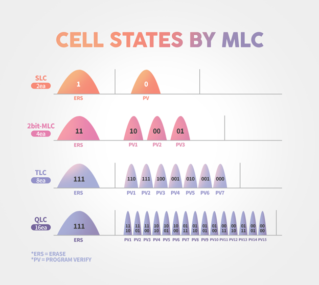
▲ Figure 1. MLC Cell States
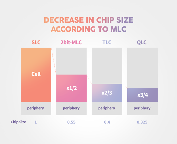
▲ Figure 2. Decrease in Chip Size according to MLC
3D/4D-NAND and Trends in the NAND Flash Industry
NAND flash memory is evolving from 2D to 3D and 4D. For 2D-NANDs, the storage capacity has increased by forming a smaller active and gate using lateral scaling to form a larger number of cells in the same area. Until the beginning of 2010, scaling in 2D-NANDs was the main focus of the technology; however, due to the limitations of fine patterning and the lifespan issue where the data is lost over time, it became no longer possible to scale. Instead, 3D-NANDs have been the main focus since the early 2010s and now all NAND manufacturers are developing and manufacturing 3D-NANDs.
3D-NANDs have a structure where storage capacity increases as the number of layers stacked through the three-dimensional stacking increases. 3D-NANDs use a method of stacking multiple layers of oxide-nitride, forming a vertical deep hole called a “plug” thereon, and then forming a memory device made of oxide-nitride-oxide therein. Through this method, a large number of cells can be simultaneously formed through a small number of processes. In a 3D-NAND, current flows through a polysilicon channel located at the center of a cylindrical cell, and program and erase information are stored according to the type of the charge stored in the silicon nitride. While forming a smaller cell was the goal of the technological development in the 2D-NAND, the core technology for the 3D-NAND is to realize three-dimensional stacking with a higher number of layers.
Recently, to further maximize the storage capacity following the 3D-NANDs, SK hynix has developed a 4D-NAND which can make the chip size even smaller. 4D-NANDs form a peripheral circuit under the 3D-NAND cell to eliminate the area occupied by the peripheral circuit, resulting in the maximization of storage capacity and lower cost of NAND flash. Over the generations, the industry increases the number of layers to store more information. The industry’s leading companies including SK hynix have already completed the development and production preparations of products up to 128 layers, and even products with a larger number of layers are under development.
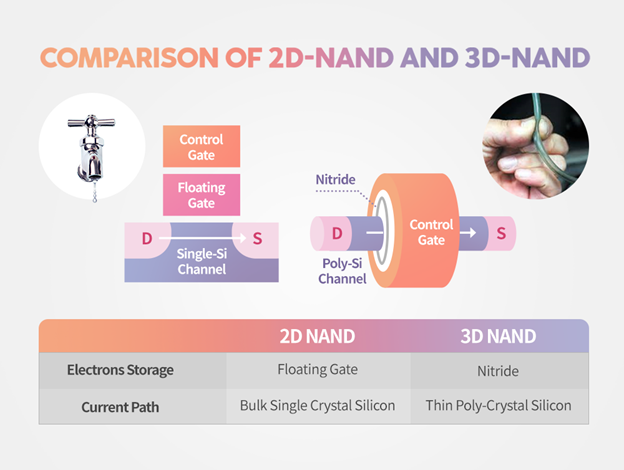
▲ Figure 3. Comparison of 2D-NAND and 3D-NAND
SK hynix’s Efforts in NAND Flash Technology
SK hynix presented a new 4D-NAND platform that maximizes storage capacity by forming peripheral circuits under the cell, using the periphery under cell (PUC) technology in the 96-layer, which is the 5th-generation 3D NAND, for the first time in the industry. In addition, SK hynix developed the industry’s first 6th-generation 128-layer product by applying the same platform, demonstrating its technological prowess in 4D-NANDs and effectiveness of the Tech Platform strategy.
The SK hynix’s 6th-generation 128-layer NAND flash features increased productivity by 40% through a 33% increase in the number of layers compared to the previous one. The random read performance was highly improved by implementing the plane interleave technology without compromising the chip area thanks to the PUC technology. In addition, the power consumption was also improved by more than 30% compared to the existing product.
In the background of this, there exists the Tech Platform strategy. While this strategy increases only the number of layers to enhance the capacity, it minimizes its development speed and investment costs by maintaining the same structure and technology. In other words, this strategy is optimal for 4D-NANDs where the capacity is enhanced by increasing only the number of layers while maintaining the same cell size. SK hynix is accelerating the development of the 7th-generation and other following products by applying this strategy to continue its technological leadership in the NAND flash sector.
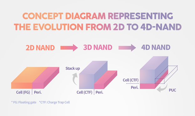
▲ Figure 4. Concept diagram representing the evolution from 2D to 4D-NAND
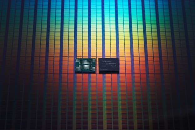
▲ Figure 5. 128-layer 1Tb TLC NAND flash
Explosive Growth for NAND Flash
NAND flash is showing explosive growth with servers including mobile and data centers. In response to this, NAND flash technology has evolved from 2D NANDs to 3D-NANDs, and then 4D-NANDs. Technologies for NAND flash are being developed to increase the storage capacity, accelerate the write and read speed, decrease the power consumption, and reduce the cost. SK hynix, a leading developer of the 4D-NAND technology, will maintain its leadership in the NAND flash evolution in the future and provide a better experience to customers with its high-performance, low-power NAND flash memory.

SangHyun Oh
Fellow, Head of NAND Platform Management at SK hynix Inc.