SK hynix has solidified its AI memory leadership, thanks in large part to its HBM — a high-performance product offering rapid processing speeds by vertically stacking DRAM chips. Behind the development of the world’s first and highest-performing HBM, and SK hynix’s top position in the AI memory market, lies the company’s unique ‘one-team’ spirit.
This second installment of the One-Team Spirit series revisits the moments when the company’s true one-team spirit fueled innovation in HBM technology, highlighting the successes, setbacks, and collaborative achievements that shaped the product.
16 Years and Counting: SK hynix’s Dedication to HBM
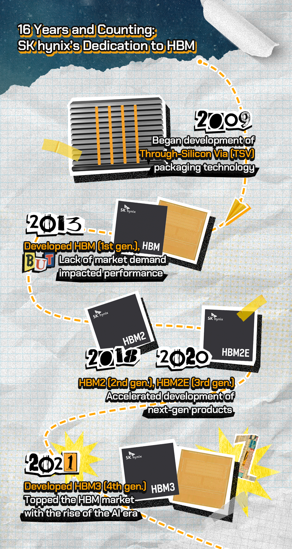
It all began in the mid-2000s with the emergence of TSV1 technology. TSV was highlighted as a potential breakthrough to overcome the limitations of memory performance and process scaling for HBM implementation. However, due to the immense infrastructure requirements and the uncertainty of success, few companies were willing to take the risk. The industry remained hesitant, opting to wait and see. SK hynix, however, was the first to act. Anticipating the impact of back-end technologies such as TSV and WLP2, the company began development of HBM in 2009. This marked the beginning of the company’s dedication to HBM, which now stands at 16 years and counting.
1Through-silicon via (TSV): A technology that drills thousands of micro-holes in DRAM chips to vertically connect the holes of upper and lower chips with electrodes.
2Wafer-level package (WLP): Technology that produces end products by packaging and testing a wafer all at once before the wafer is diced. It differs from the conventional packaging method of processing a wafer and dicing each chip.
The full-scale application of TSV began in 2013. Around this time, demand was growing for high-performance, near-memory3 solutions for GPUs. SK hynix leveraged TSV and WLP to launch the world’s first HBM. However, the market was not quite ready for such a product. The high-performance computing (HPC) ecosystem had not yet matured, and the product’s early arrival posed challenges for broad adoption. Facing market limitations and reduced expectations, SK hynix’s HBM development department faced a defining moment.
3Near-memory: Memory located close to the computing unit (processor), enabling faster data processing.
Nonetheless, the company remained steadfast in its commitment to HBM. There was a firm belief that the HPC era would soon arrive, and the company that created the best product would seize the advantage. Moreover, it was impossible to abandon HBM considering the vast technological prowess which had already been accumulated at the company. As a result, SK hynix employees united once again with the goal of developing the highest-performing HBM.
In 2020, the tide finally turned. The company’s perseverance with HBM2E, the third generation of HBM, and HBM3, the fourth-generation HBM, paid off as the AI era gained momentum, sparking demand for AI and HPC applications. Armed with years of technological expertise, SK hynix rapidly expanded its market share and claimed the No. 1 position in the HBM market. This hard-won achievement was the result of 16 years of strategic foresight, relentless innovation, and a ‘one-team’ spirit — uniting front-end teams driving DRAM chip development with back-end teams advancing packaging technologies such as TSV.
World’s Best HBM3E: Making the Impossible Possible With One Team’s Strength
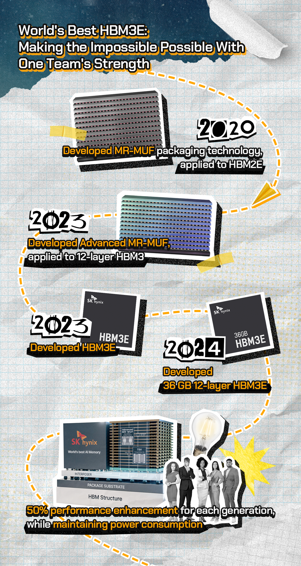
Securing the market lead with HBM2E was just the beginning. In 2021, SK hynix solidified its No. 1 position with the launch of HBM3. Capable of processing 819 GB of data per second, the product was a clear demonstration of the company’s technological edge. SK hynix also set a new industry benchmark by increasing the number of DRAM chip stacks, culminating in the release of the 36 GB 12-layer HBM3 in April 2023.
Just four months later, in August 2023, SK hynix made headlines again by announcing the fifth generation of HBM, HBM3E. With a rapid data processing speed of 1.15 TB per second, HBM3E quickly gained dominance in the AI memory market.
A key enabler of SK hynix’s HBM success was its proprietary MR-MUF4 technology, first applied to HBM2E. This advanced packaging technique enhanced performance, improved heat dissipation, and enabled high-volume production. The innovation continued with Advanced MR-MUF, applied to the 12-layer HBM3. This updated technique allowed for thinner chip stacking without warpage and used new protective materials to optimize thermal performance, positioning SK hynix’s HBM as a premium solution.
4Mass reflow-molded underfill (MR-MUF): A process in which a liquid protective material is injected between the spaces of stacked chips before hardening to protect the circuits. MR-MUF offers more efficient and effective heat dissipation compared to the method of laying a film material between each chip.
At the core of the company’s HBM development was an ambitious goal: to improve performance by 50% with each generation while maintaining the same power consumption. Achieving this required close collaboration across departments, from packaging to HBM development, where experts from diverse fields worked side by side to solve technical challenges in real time. SK hynix’s HBM3E was the result of this seamless one-team cooperation.
Capturing the Global AI Market With One-Team Spirit

SK hynix’s dominance in the global AI memory market continued into 2025. In March, the company became the first in the world to supply samples of the 12-layer HBM4, the sixth-generation HBM, marking a major milestone built on 16 years of technological expertise.
Despite the increased complexity, SK hynix shortened the development timeline while achieving industry-leading performance. With a data processing speed of 2 TB per second, HBM4 can process over 400 Full HD movies, each with a capacity of 5 GB, in just one second — a 60% speed increase from the previous generation. Once again, the company met its ambitious goal of improving performance by more than 50% with each new generation.
The driving force behind this breakthrough was the company’s unwavering ‘one-team’ spirit. Employees worked in unison across departments, sharing knowledge and solving challenges collaboratively. This spirit of unity extended beyond the company, as SK hynix strengthened partnerships by incorporating a global foundry’s logic processes into the HBM base die. This is expected to further enhance both performance and power efficiency.
Mass production of HBM4 is scheduled to begin in the second half of 2025. Through this, SK hynix aims to reinforce its technological leadership and further cement its position in the AI memory space. With HBM4 poised to make a significant market impact, expectations are high for how far SK hynix can expand the AI memory frontier.


