Continuing from the previous episode which introduced conventional and wafer-level packages, this article will explore packaging technologies that combine multiple packages and components within a single product. In particular, it will explain package stacking and system-in-package (SiP) technologies which reduce the required development space and increase the efficiency of the packaging process.
Stacked Packages
Imagine a housing complex consisting of numerous low-rise buildings for thousands of people. It would require a very large area to accommodate the residents. However, the same number of residents could fit in a single skyscraper. This example clearly shows one of the key benefits of stacked packages. Compared to a product made with multiple packages spread horizontally across a wide area, a product consisting of stacked packages offers enhanced performance within a much smaller space. In addition to being an important packaging technology, stacked packaging is also an essential method in product development.
It used to be common for products to have only one chip per package, but it is now possible to develop a multi-chip package that has different functions or to place multiple memory chips in a single package that has an increased capacity. Furthermore, the development of SiP has allowed various system components to be implemented in a single package. Such technologies have enabled semiconductor companies to create high value-added products while also responding to the diverse needs of the market.
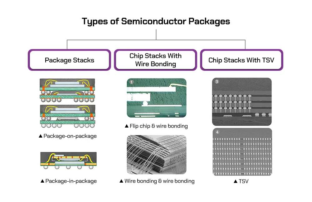
▲ Figure 1. Different methods of stacking packages (Source: Hanol Publishing)
As Figure 1 shows, stacked packages are categorized into three major types based on their distinct development techniques: 1) package stacks that are made by vertically stacking the packages, 2) chip stack packages that use wire bonding to stack chips within a single package, and 3) chip stack packages that use through-silicon via (TSV)* rather than traditional wire bonding for the internal electrical interconnections. Each of these stacked packages has different features and various advantages and limitations which will determine their future applications.
* Through-silicon via (TSV): A type of vertical interconnect access (via) that completely passes through a silicon die or wafer to enable the stacking of silicon dice.
#1. Package Stacks
A package stack is made by vertically stacking the packages. Consequently, its advantages and disadvantages are opposite to that of chip stack packages. The package stack method places packages on top of each other once they have completed testing, so it is possible to easily replace a package that fails a test with a properly functioning package. This, in turn, results in better test yields compared to chip stack packages. However, due to package stacks’ larger size and longer signal paths, their electrical characteristics can be inferior to that of chip stack packages.
One of the most common package stacking methods is package-on-package (PoP), which is widely used in mobile devices. For a PoP in a mobile device, the types and functions of the chips used in the upper and lower packages may vary while the chip manufacturers can also differ.
In general, the upper packages mainly include memory chips made by semiconductor memory companies while the packages stacked below feature chips with a mobile processor that are designed by fabless companies and produced in foundries and Outsourced Semiconductor Assembly and Test (OSAT) facilities. As the packages are manufactured by different parties, quality testing is conducted before being stacked. Even if a defect occurs after stacking, it can be reworked by just replacing the defective part with a new package. Accordingly, it is clear that the mobile business sees significant benefits from package stacking.
#2. Chip Stacks with Wire Bonding
When placing multiple chips in a package, they can either be stacked vertically or attached horizontally to the board. Given that the horizontal layout may result in a larger package size, vertical stacking has become the preferred method. Compared to package stacks, chip stack packages are smaller in size and possess enhanced electrical characteristics due to their shorter electrical signal paths. However, even if a defect is found in a single chip during testing, the entire package needs to be discarded. Thus, chip stack packages have relatively low test yield rates.
In chip stack packages, the memory capacity increases as more chips are stacked in the package. This has resulted in the development of technologies which enable more chips to be layered in a package. However, as it is undesirable for the package to get thicker even as more chips are stacked, technologies that limit the package’s thickness have been under development. To do so, everything that affects the thickness of a package including the chip and the substrate must be made thinner, and the gap between the uppermost chip and the surface above the package needs to be reduced. This poses many challenges in the packaging process because chips are more likely to get damaged as they become thinner. That is why developments in packaging processes are underway to overcome these challenges.
#3. Chip Stacks with TSV
TSV is a chip stacking technique that drills holes through silicon to accommodate electrodes. Instead of using the traditional method of wiring to connect chip-to-chip or chip-to-substrate, TSV connects chips vertically by drilling holes in the chip and filling them with conductive materials such as metal. Although a chip-level process is used when stacking with TSV, a wafer-level process is used to form TSV and solder bumps on the front and back of the chip. Therefore, TSV is classified as a wafer-level package technology.
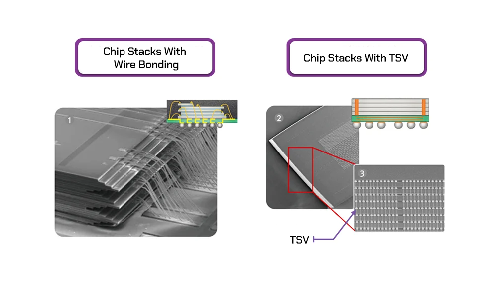
▲ Figure 2. A cross-sectional view of a chip which applied TSV technology (Source: Hanol Publishing)
The main advantages of packages using TSV are the high level of performance and smaller package size. As shown in Figure 2, the chip stack package with wire bonding has wires connected to the sides of each stacked chip. As there are more stacked chips and connected pins, the wiring becomes more complex, with more space needed to connect them. In contrast, the chip stack with TSV does not require complicated wiring and, therefore, allows reduction in package size.
As explained in the previous episode, flip chips have good electrical properties due to several reasons: it is easier to form I/O pins in desired locations, there is an increase in the number of pins, and they have short electrical signal transmission paths. These are the same reasons that give TSV packages strong electrical properties. When sending an electrical signal from a chip to the chip right below it, TSV allows the signal to go straight down. In contrast, if wire bonding is used, the signal transmission path becomes much longer as the signal has to go down to the substrate before making its way up to the chip. As shown in the image of a chip stack with wiring in Figure 2, wiring connections cannot be made in the center of the chip. Contrastingly, TSV packages allow the center of the chip to be drilled, made into electrodes, and connected with other chips. Unlike wiring connections, TSV enables the number of pins to be significantly increased.
High Bandwidth Memory (HBM) utilizes a new DRAM architecture that takes advantage of this ability to increase the number of pins. Typically, an “X4” in DRAM specification implies that there are four pins that can send information, or 4 bits of information can be simultaneously sent from the DRAM. Accordingly, X8 refers to 8 bits, X16 refers to 16 bits, and so on. It is favorable to increase the number of these pins as it allows more information to be sent simultaneously. However, chip stacking with wiring could only reach X32 due to limitations, while stacking through TSV does not have such limitations, enabling HBM to go up to X1,024.
Current mass-produced memory products that apply TSV to DRAM include HBM and 3D stacked memory (3DS). The former is used in graphics, networking, and high-performance computing (HPC) applications, while the latter is primarily used as a DRAM memory module.
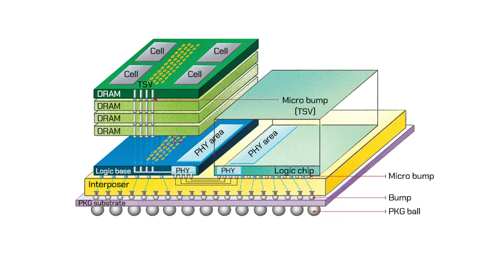
▲ Figure 3. A 2.5D package using HBM (Source: Hanol Publishing)
Rather than being a fully packaged product, HBM is a semi-packaged product. When an HBM product is sent to a system semiconductor manufacturer, they use an interposer* to make a 2.5D package* , with an HBM placed side-by-side to a logic chip as shown in Figure 3. Since substrates in 2.5D packages are unable to provide pads that can support all the I/O pins of both HBMs and logic chips, interposers come in to accommodate HBMs and logic chips by creating pads and metal wiring. Then, these interposers connect back with the substrate. As for these 2.5D packages, they are considered as a type of SiP.
3DS memory, another product that uses TSV, is a type of memory module with a BGA* package mounted on a PCB board. Although DRAM memory modules in servers require high speed and a large capacity, chip stack packages that use wiring are unable to meet these requirements due to their speed limitations. This has led to the use of modules made from TSV-applied chip stack packages for high-end systems such as servers.
* Interposer: Wide and extremely fast electrical signal conduits used between die in a 2.5D configuration.
* 2.5D package: 2.5D and 3D packages include multiple integrated circuits inside each package. In the 2.5D structure, two or more active semiconductor chips are placed side-by-side on a silicon interposer. In the 3D structure, active chips are integrated by die stacking vertically.
* Ball grid array (BGA): A type of surface mount chip package that uses a grid of solder balls as its connectors.
System-In-Package (SiP)
A package consisting of HBM and a logic chip is a type of SiP. As its name suggests, SiP implements a system in a single package. While components such as sensors, analog-to-digital (A/D) converters, logic chips, memory chips, batteries, and antennas must also be included to form a complete system, it is not possible to include all these system components into a single package with the current developments in technology. It has therefore become the goal of researchers to continue developing package technologies in this area, and SiPs today usually refer to combining some of the system components in a single package. For instance, packages that have applied HBM combine HBM and the logic chip into a single package to create an SiP.
Unlike SiP, system-on-chip (SoC) implements system functions on the chip-level. In other words, several system functions are implemented on one chip. As an example, most processors today have static RAM (SRAM) memory within the chip, allowing the logic functions of the processor and the memory functions of the SRAM to be implemented together on a single chip. Therefore, these processors are classified as an SoC.
SoCs have a complex and lengthy development process because they require multiple functions to be packed into a single chip. Moreover, upgrading the functions of a single element in an already developed SoCs requires one to design and develop them from scratch. SiPs, on the other hand, are easier and quicker to develop because they are made by collecting already developed chips and devices into a single package. Even if the device has a completely different structure, the chip itself is developed and manufactured separately, making it relatively easy to make it into a single package. Also, if just a single aspect of the function needs an upgrade, the newly developed device can be implemented in the chip without developing the whole package from scratch. However, if a product is going to be used in large quantities over an extended period of time, it may be more efficient to develop it as an SoC rather than an SiP as the latter requires more materials to be manufactured and leads to a larger package size to fit multiple chips in a single package.
Despite the various differences between SoCs and SiPs, it is not necessary to choose between one of these two technologies. In fact, they can be combined to create synergies. Once an SoC is developed, it can be packaged with other functional chips into a single package and implemented as an enhanced SiP.
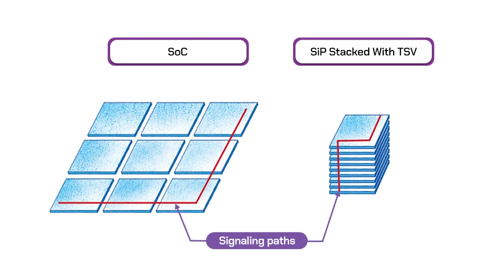
▲ Figure 4. Comparison of signal transmission path length of SoC and SiP stacked with TSV (Source: Hanol Publishing)
When comparing the performance of SiPs and SoCs, it was originally thought that the electrical characteristics of SoCs were better due to their implementation on a single chip. However, with the advent of chip stacking technology such as TSV, SiPs can have electrical characteristics that are on par with SoCs. Figure 4 shows a comparison of the signal transmission paths of SoCs and SiPs stacked with TSV. When a signal is transmitted from one end of an SoC chip to the opposite corner, the path is much shorter if the SoC is divided into nine parts and stacked with TSV.
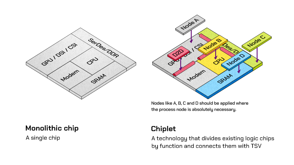
▲ Figure 5. Conceptual diagram of a chiplet
In addition to a focus on the various advantages of SiPs stacked with TSV, a technology called chiplets has gained a lot of attention recently. As shown in Figure 5, it is a technology that divides existing logic chips by function and connects them with TSV. Chiplets have three main advantages over monolithic chips.
First, the chiplets offer a yield improvement over monolithic chips. The wafer yield is limited if the size of a single chip on the wafer is big, but making the chips smaller can increase wafer yield and thus reduce manufacturing costs. Take the example of a 300 mm wafer cut into 100 or 1,000 chips (net die). If the wafer process causes five chips to fail because five impurities are evenly distributed across the front of the wafer, the product with 100 chips has a yield of 95% and the product with 1,000 chips has a yield of 99.5%. The yield is therefore much higher for products with more net dies, or with a smaller chip size. Therefore, it is more cost-effective to cut up a chip by functions and implement it as SiP rather than as a single chip through SoC.
The second advantage is streamlined development. With a single chip, the entire chip needs to be redeveloped in order to upgrade its functionality or apply the latest technology. However, dividing the chips can shorten the development period and make the process more efficient as only the chip with the relevant function needs to be upgraded or developed with the latest technology. For example, some of the segmented chips use the existing 20 nanometer (nm) technology, while others use the latest sub-10 nm technology to increase development efficiency.
The third benefit is the centralization of technological development. By dividing chips by function, it is not necessary to develop a chip for every function. Only the chips used for the core technology need to be developed, and everything else can be purchased or outsourced so companies can focus on developing their own core technologies.
Thanks to these advantages, major semiconductor companies are introducing chiplet-based semiconductor products or have added them to their roadmaps.
Following the previous episode that looked into the various conventional and wafer-level packaging technologies, we finished the roundup of packaging technologies and their distinct characteristics. While stacked packages and SiPs have come a long way in their development, semiconductor researchers will continue efforts to enhance the capability of these high-quality technologies with numerous functions that take up a minimal amount of space. These efforts are expected to increase the efficiency of the packaging process as a whole through the production of packages with advantages in size, functionality, and performance.