

Following an introduction to the basic process of assembling a wafer-level package in the previous episode, this article will go over the multiple process stages of different types of wafer-level packages. These include the fan-in wafer-level chip-scale package (WLCSP), fan-out WLCSP, redistribution layer (RDL) package, flip chip package, and through-silicon via (TSV) package. Additional wafer-level processes that are applied in these packages such as photolithography, sputtering, electroplating, and wet processes will also be explained.
Fan-in Wafer-Level Chip-Scale Package (WLCSP) Process
In a fan-in WLCSP, a tested wafer enters the packaging line and a layer of metal film is created using sputtering. A thick layer of photoresist is then applied to the metal film as the photoresist must be thicker than the metal wiring used for packages. Photolithography is used to form patterns on the photoresist, and these exposed areas are copper electroplated to form the metal wiring. Next, the photoresist is stripped, and the excess thin metal film is removed using chemical etching. A dielectric layer is then formed on top, and photolithography is used to remove only the areas where the solder balls will be placed. Thus, this layer is also referred to as “solder resist.” It serves as the WLCSP’s passivation layer, or final protective layer, and distinguishes the area where the solder ball will be placed. Without this layer, solder balls would continue to melt on top of the metal layer and would not retain their globular shape when they are attached using methods such as reflow soldering.
Solder balls are attached to the dielectric layer through solder ball mounting after the layer forms a pattern through photolithography. Once the solder balls are mounted, the packaging process is complete and individual fan-in WLCSPs can then be created by dicing the wafer.
Solder Ball Mounting Process
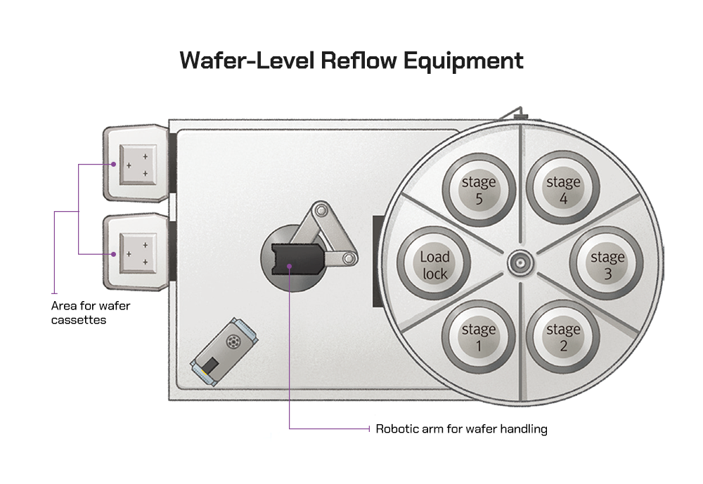
▲ Figure 1. A bird’s eye view of wafer-level reflow equipment (Source: Hanol Publishing)
The process of solder ball mounting involves attaching solder balls onto a WLCSP for packaging. The key distinction from placing solder balls on a substrate in conventional packaging lies in the fact that solder balls are placed atop a wafer. Thus, flux application, solder ball mounting, and the reflow process follow the same steps, except that the stencil utilized to applying flux and mounting solder balls has the same size as the wafer itself.
Additionally, the reflow equipment takes a hot plate-based approach, as depicted in Figure 1, as opposed to the convection reflow method involving conveyers. In wafer-level reflow equipment, different temperatures are applied to wafers as they progress through the various stages. This ensures that packaging can progress while maintaining a temperature profile for the reflow process.
Flip Chip Bump Process
The process of forming bumps in a flip chip package is carried out in the wafer-level process, while the subsequent steps are conducted in the conventional packaging processes.
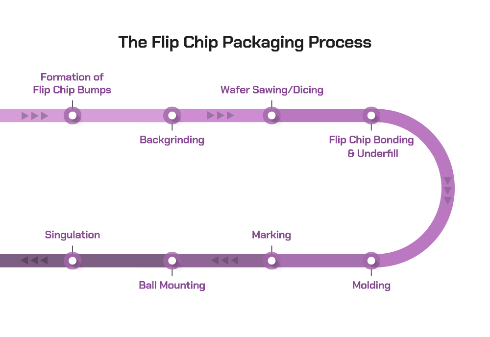
▲ Figure 2. An overview of the flip chip packaging process
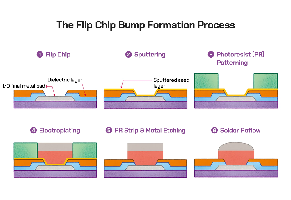
▲ Figure 3. The steps for forming a flip chip bump
As the bumps must be sufficiently high, it is necessary to select a photoresist that can be thickly applied to the wafer-level package. Copper pillar bumps (CPB)1 are formed through copper plating followed by solder plating. This solder is typically a lead-free tin/silver alloy. Once plating is complete, the photoresist is removed and the under bump metallurgy (UBM)2 film formed by sputtering is removed via metal etching. The bumps are then molded into a spherical shape using wafer-level reflow equipment. The solder bump reflow process here serves to minimize height discrepancies among the bumps, reduce the surface roughness of the solder bumps, and eliminate oxides from the solder, all of which enhance the bonds during the flip chip bonding process.
1Copper pillar bump (CPB): The structure of the bump for flip chip bonding to reduce the gap between the bumps. Copper is used to form the pillars that have bumps on top of them.
2Under bump metallurgy (UBM): The metal layer formed under flip chip bumps.
Redistribution Layer (RDL) Process
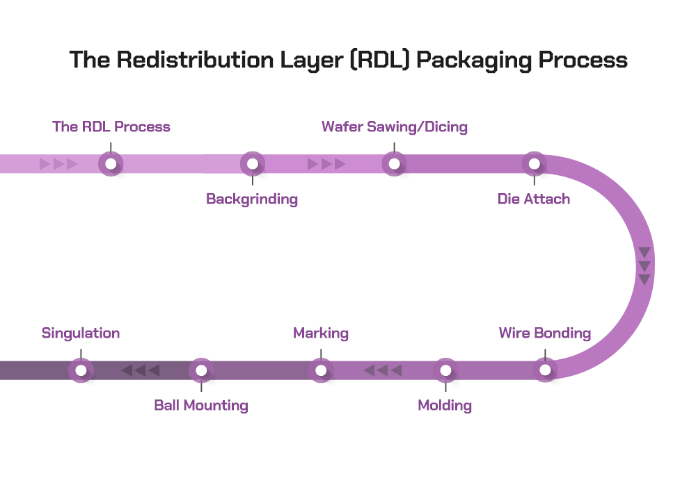
▲ Figure 4. An overview of the packaging process using a redistribution layer (RDL)
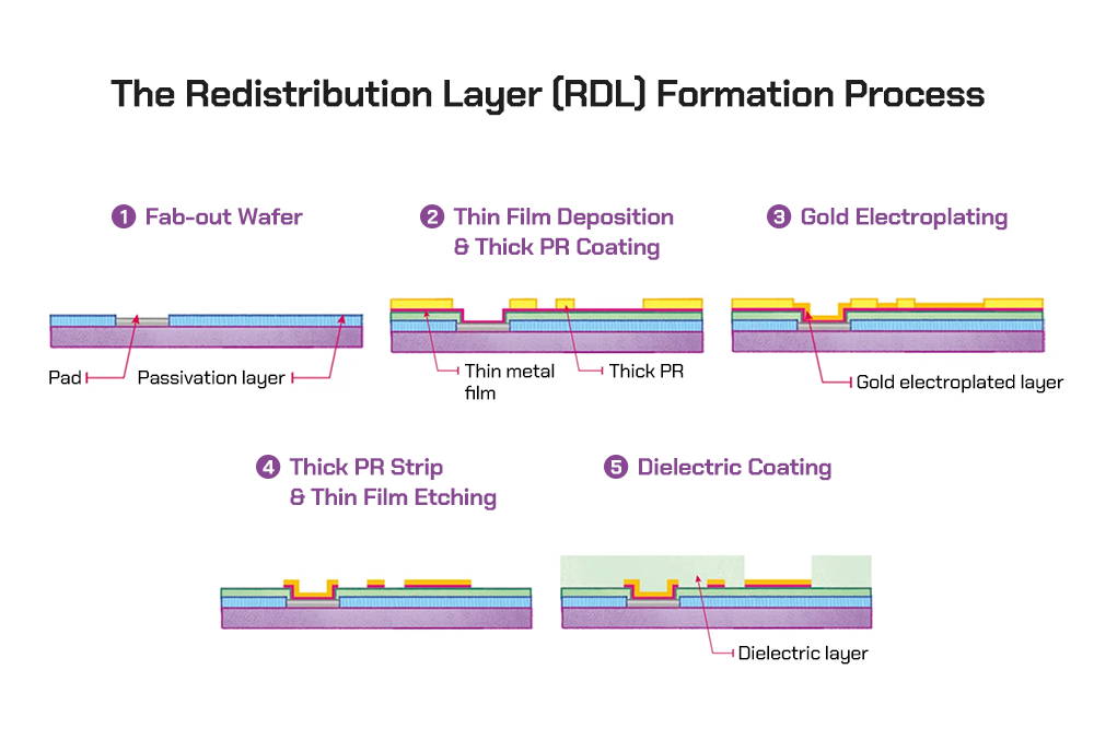
▲ Figure 5. The steps for forming a redistribution layer (RDL)
Used for chip stacking, the redistribution layer (RDL) process creates a new pad by forming an extra layer of metal wiring over a pad formed on a wafer. Consequently, the packaging processes after the RDL process follow conventional packaging processes, as depicted in Figure 4. During chip stacking, the die attach and wire bonding steps are repeated equally for each chip that needs to be stacked.
In the RDL process, sputtering is first used to create a thin layer of metal film, which is covered with a thick layer of photoresist. A pattern is created through photolithography so that the exposed areas of the pattern can be electroplated with gold to form metal wiring. Since redistribution itself is a process of rebuilding the pad, the ability to form strong bonds is essential for wire bonding. This is why gold, which is widely applied for wire bonding, is used for plating.
Fan-out Wafer-Level Chip-Scale Package (WLCSP) Process
The process of fabricating a fan-out WLCSP begins by applying tape to a wafer-shaped carrier. After wafer dicing, the high-quality chips are attached on top of the tape at regular intervals. The spaces between the chips are filled with wafer molding, resulting in a new shape. Once the wafer molding is complete, the carrier and tape are removed. Next, metal wiring is created on the newly formed wafer using wafer equipment, followed by the attachment of solder balls for packaging. Finally, the wafers are diced into individual packages.
Wafer Molding
To create a fan-out WLCSP, wafer molding is an essential step. The wafer molding process entails placing a wafer—in the case of a fan-out WLCSP, a wafer-shaped carrier with chips attached to it—into a molding frame. An epoxy molding compound (EMC)3, which can be in the form of a liquid, powder, or granules, is then added to the frame and compression and heat are applied to mold the setup. Wafer molding is not only an essential process for fan-out WLCSPs, but it is also a requirement for a known good stacked die (KGSD)4 that uses TSV, which will be discussed later.
3Epoxy molding compound (EMC): A heat dissipation material based on an epoxy resin, or a type of thermosetting polymer. It seals semiconductor chips to protect them from external environmental factors such as heat, moisture, and shock.
4Known good stacked die (KGSD): A product comprised of stacked chips that have been tested and confirmed to be of good quality. A prime example is HBM.
Through-Silicon Via (TSV) Package Process
Figure 6 illustrates the process steps of fabricating a TSV package using a via-middle5 approach. First, vias are formed during wafer fabrication. Subsequently, solder bumps are formed on the wafer’s front side during the packaging process. The wafer is then attached to a carrier wafer and backgrinded. After bumps are formed on the backside of the wafer, the wafer is diced into units of chips and stacked.
5Via middle: A type of TSV that fabricates TSVs after the formation of CMOS but before the metal layers are formed.
To provide a brief overview of the process of forming TSVs with middle vias, transistors such as CMOS are initially fabricated on a wafer during the front-end of line (FEOL) process. Then, using a hard mask (HM)6, a pattern is created where the TSV will be formed. Next, the areas without the hard mask are removed through dry etching to create deep trenches. Insulating films, such as oxides, are subsequently deposited via chemical vapor deposition (CVD). This insulating film serves to isolate metals like copper that will later fill the trenches, preventing the metals from contaminating the silicon. Additionally, a thin layer of metal that acts as a barrier is created atop the insulating film.
6Hard mask (HM): A mask that creates finer patterns as it is made up of harder materials than soft masks. Since an HM is not photosensitive in itself, additional patterning needs to be formed with the application of photoresist, followed by the subsequent etching process.
This thin layer of metal is used to electroplate copper. After electroplating, the wafer’s surface is smoothed through chemical mechanical polishing (CMP), which simultaneously eliminates all of the copper from the surface of the wafer, ensuring that copper remains solely within the trenches. This is followed by the back-end of line (BEOL) process to complete the wafer fabrication.
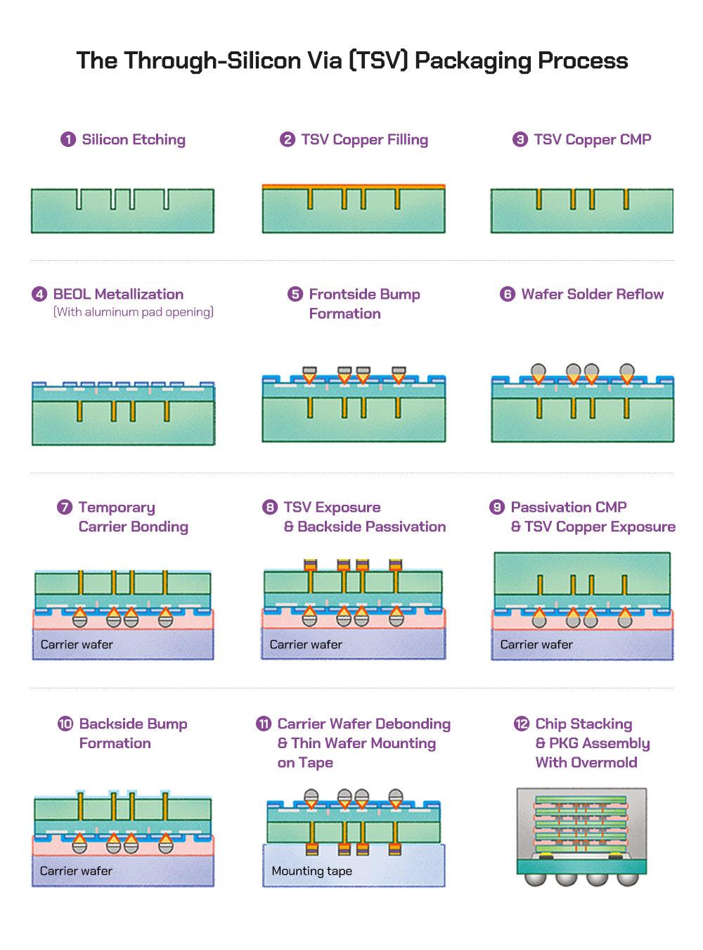
▲ Figure 6. The steps of the TSV packaging process (Source: Hanol Publishing)
There are two main types of packages that can be created when producing chip stack packages using TSV technology. The first is a package that uses a substrate with 3D chip stacking technology. The second type involves creating a KGSD and then using it to make a 2.5D or 3D package. The following section will explain the processes of fabricating KGSDs and using them to create 2.5D packages.
As a chip stack package which uses TSV, KGSD has to undergo additional packaging processes such as 2.5D packaging, 3D packaging, and fan-out WLSCP. A prime example of a KGSD product is high bandwidth memory (HBM). Since a KGSD needs to go through additional packaging processes, the connection pins are formed as fine solder bumps rather than conventional solder balls. As a result, while chips in a 3DS package are stacked on a substrate, chips in a KGSD are stacked on a wafer, which also serves as the bottommost chip of the KGSD. In the case of HBM, the chip at the bottom is referred to as the base chip or base wafer, while the chips stacked above it are known as the core chips.
To explain the process steps, bumps are formed on the front surface of both the base and core wafers through a flip chip process. In the context of a 2.5D package, the base wafer necessitates the arrangement of bumps so that they can be attached to interposers. Conversely, the core wafer forms a bump layout that facilitates chip stacking on the front of the wafer. After bumps are formed on the frontside of the wafer, the wafer should be thinned, and bumps should also be formed on the wafer’s backside. However, as previously mentioned during the introduction of the backgrinding process, it is important to note that thinning the wafer can induce the wafer to warp. While conventional packaging makes it possible to have wafers taped to ring frames following the backgrinding to prevent wafer warpage, this method is not viable in TSV packaging where bump formation occurs on the wafer’s backside. This is exactly why the wafer support system (WSS) was developed. Under the WSS, the frontside of the wafer with bumps is bonded to a carrier wafer with a temporary adhesive. At the same time, the backside of the wafer is grinded to thin it. Since it is attached to the carrier wafer, the thinned wafer does not warp.
Additionally, since the carrier wafer is also in the form of a wafer, it can be processed using wafer equipment. Using this structure, bumps are created on the core wafer’s backside. Once bumps are formed on both sides of the core wafer, the carrier is debonded. Then, the wafer is taped to a ring frame and diced in the same manner as conventional packaging processes. The base wafer remains attached to the carrier wafer as it removes chips that are diced from the core wafer to stack on top of the base wafer. When chip stacking is complete, the base wafer is molded while the carrier wafer is debonded. In this way, the base wafer becomes a molded wafer with core chips stacked on it. This wafer is grinded to the target thickness suitable for making a 2.5D package and then diced into chips to form KGSDs. This finished HBM is packed and shipped to customers who will make 2.5D packages.
Wafer Support System (WSS) Process
A WSS refers to a system that allows further processing on the backgrinded surface of a thinned wafer. This process occurs prior to the completed backgrinding process. The WSS process involves two main steps: carrier bonding, which involves attaching a carrier to a wafer for TSV packaging; and carrier debonding, where the carrier is detached after completing processes like forming bumps on the wafer’s backside.
Figure 7 depicts the WSS process steps, where carrier bonding involves applying a temporary adhesive to the wafer before attaching it to the carrier. Carrier debonding involves removing the carrier after processes on the backside are completed and ensuring the wafer is cleaned to remove any residual adhesive.
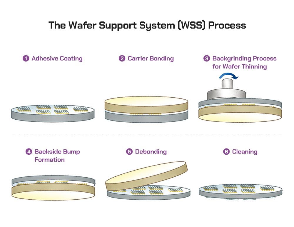
▲ Figure 7. The steps of the wafer support system (WSS)
There are several considerations to be taken into account in carrier bonding: the overall thickness of the wafers bonded through carrier bonding should be uniform; there should be no voids at the bonded joints; the alignment of the two wafers should be accurate; there should be no adhesive-related contamination at the edge of the wafers; and wafer warpage should be minimized during the process. During the carrier debonding, there should also be: no damage such as chipping7 or cracking to the wafer that is separated from the carrier; no adhesive residue; and no deformation of the bumps.
7Chipping: The breaking of the edges or corners of a chip or wafer.
Debonding stands out as a relatively complex and critical step within the WSS process. As a result, various debonding methods have been proposed and developed, accompanied by the development of different temporary adhesives for each method. Typical methods include thermal techniques, laser ablation followed by peel-off, chemical dissolution, and chemical cleaning after mechanical lift-off.
Wafer Edge Trimming Process
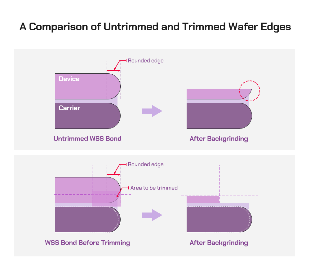
▲ Figure 8. A comparison of the edges of untrimmed (upper image) and trimmed (lower image) wafers
After a wafer for a TSV package is bonded to a carrier wafer and then backgrinded, it will have sharp edges, as shown in the red circle in the upper image of Figure 8. In this state, the wafer undergoes subsequent processes such as photolithography, metal film formation, and electroplating to form bumps on the backside. However, these processes elevate the risk of chipping the wafer’s edge. Cracks at the edge could propagate inward, eventually rendering further processing impossible, thereby resulting in significant yield loss. To preemptively overcome this problem, the edge of the frontside of the wafer designated for TSV packaging is trimmed and removed before it is bonded with the carrier wafer. When the trimmed wafer is bonded to the carrier wafer and backgrinded, the sharp edge’s prominence diminishes, as shown in the lower part of Figure 8. Consequently, the risk of chipping during subsequent processes is eliminated. The trimming process employs a rotating wafer dicing blade that traverses the wafer’s edge, removing a designated segment of the edge.
Stacking Process
In TSV packaging, the bumps formed on the front and back of wafers are bonded together for stacking. Like in flip chip bonding, mass reflow (MR) and thermocompression are used for bonding. Depending on the type of stacking, the processes are classified as chip-to-chip stacking, chip-to-wafer stacking, and wafer-to-wafer stacking.
When stacking chips with TSVs, micro bumps are used. Therefore, the gaps between these bumps are small, as is the spacing between stacked chips. This is why thermocompression, known for its high reliability, has been widely adopted. However, thermocompression has the disadvantages of taking a long time and has low productivity as heat and pressure must be applied for a certain period during bonding. As such, there’s a growing trend toward adopting MR as an alternative bonding technique.
Looking Beyond the Types of Wafer Packaging
After discussing the two main groups of conventional and wafer-level packages in these two last episodes, the next chapter in our series will delve into the materials that make up the various components of these packages. In particular, it will cover the unique properties of these small materials and analyze how they affect the performances of these semiconductor products.


