In this final episode of our series on front-end processes, we will introduce the process of metallization which connects semiconductor devices using metals such as aluminum and copper. As these interconnections provide power and enable the chip’s operation, they highlight the significance of metallization in semiconductor manufacturing. This article will also introduce the role of contacts and barrier metals in metallization, and provide an insight into the larger context of connections from the perspective of a semiconductor manufacturer.
Connections: The Veins of the Semiconductor
After the processes explored in the previous episodes including oxidation, photolithography, etching, and deposition are completed, semiconductor devices are finally formed on the wafer’s surface. For memory chip makers like SK hynix, they line up transistors and capacitors* on the wafer’s surface, while foundries or CPU manufacturers line up three-dimensional transistors such as FinFETs* on the wafer.
* Capacitor: A storage battery that can store electricity and is often used for electronics. In this article, it refers to a device used to store data in a semiconductor.
* FinFET (Fin field-effect transistor): A type of three-dimensional MOSFET that has an electric current with a path that resembles a fish’s dorsal fin.
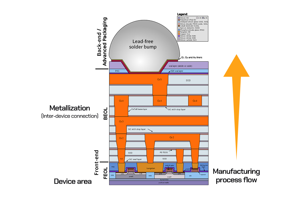
▲ Figure 1. Layers of a semiconductor device and areas of metal wiring (Image Source)
However, these devices prove to be useless if they are isolated. Just as individual devices on top of an electronic substrate cannot work unless they are soldered, transistors on a wafer cannot function without being interconnected with each other. These transistors operate by receiving external power so they can perform various tasks such as moving processed data to the next area. Accordingly, a process is required to connect devices to one another, or to a power source. As for these devices, they must interact with one another using electricity as semiconductors are essentially electronic circuits. This is where the metallization process comes in to enable the operation of a semiconductor. As for different types of semiconductors like CPUs or GPUs, they are created using the same devices that are interconnected in different ways.
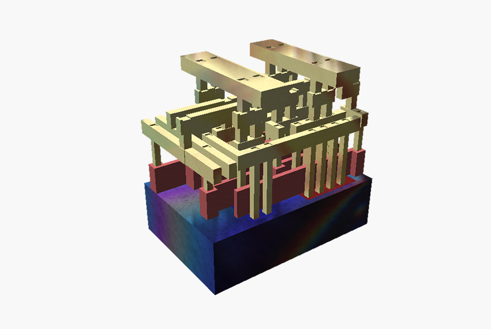
▲ Figure 2: Metal wiring (yellow) connecting the device’s layers (red). *Some structures omitted. (Image Source)
Metallization is not a single process such as photolithography, etching, and deposition—processes that make it possible to apply metal wiring on a semiconductor. Additionally, the metallization process is distinguishable for using materials, including metals, that have different characteristics from materials that were used in the previous process of forming device layers.
Thus, there is no “metallization equipment” like there is etching equipment. Instead, equipment that is used in other processes is also used to make the metal wiring in the metallization process. When a material needs to be carved out, etching equipment is used, while deposition equipment is generally used to fill empty spaces. All the while, photolithography is involved between these processes.
Contacts: Linking Wires and a Device
When connecting devices on the substrate, electric wires are first connected and then soldered on. As layers are stacked starting from the bottom on a semiconductor, a junction called a contact—which connects metal wiring with a device—is created after the formation of the bottom device layer. The wiring is then connected on top of it.
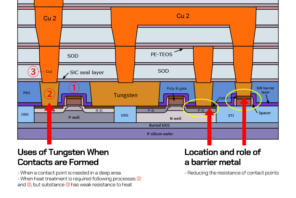
▲ Figure 3. The use of tungsten in the formation of contacts, and an example of barrier metal (Image Source)
It might seem like metal can be connected directly to the device without a contact, but an issue arises as semiconductors go through miniaturization. This problem is related to the gaps that inevitably form on the semiconductors. Although the deposition process has a “gap-fill” property that fills in these voids to prevent devices from disintegrating, metals such as aluminum are not able to fill in deep holes even with deposition. This results in faulty wires which are desolate in the middle. Due to this problem, the gap must be filled beforehand by depositing a metal like tungsten (W) that has a superior gap-fill property so the deep metal wiring can be formed. This applies when there is significant distance between the device layer and the metal layer. Otherwise, high-temperature heat treatment is required following the formation of metal contacts. Furthermore, even when a metal or a material that is not heat-resistant like aluminum is used, contacts need to be formed with tungsten while aluminum wires are placed on top.
Barrier Metals: Reducing Metal-to-Metal Resistance
Meanwhile, a metal—or metal compound—called a barrier metal is needed between the device and the contact. In semiconductor processing, it is very difficult to precisely connect non-metallic and metallic materials. When two materials with different characteristics are directly connected, a high resistance caused by the difference in conduction bands* between the metal and silicon occurs at the boundary. This leads to an increase in the power consumption of the semiconductor. To avoid this, it is necessary to add a barrier metal. To make a barrier metal, materials such as titanium (Ti) or cobalt (Co) are applied on top of the silicon layer of a semiconductor device, and the metal reacts with the silicon atoms. This process is called ‘silicidation’ while the corresponding area is known as a contact silicide.
* Conduction band: Among the two bands that are separated by an energy gap in the energy band structure of a solid, the band on top contributes to the conduction of the solid.
Barrier metals are also used to prevent unwanted damage to the device during processes. Aluminum, for example, tends to react with silicon (Si) which is the main material in wafers. When the aluminum metal wiring closely passes by the silicon in the device layer, a barrier metal such as a titanium compound needs to be placed between the two as a barricade.
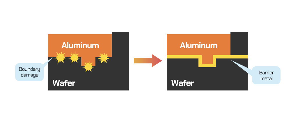
▲ Figure 4. The purpose of the barrier metal when using aluminum wiring
In addition, the increased use of copper conductors due to the limitations of aluminum has resulted in further application of barrier metals. Unlike aluminum, copper has the tendency of diffusing into silicon dioxide (SiO2) which is more stable than silicon. If left unchecked, the oxide film that is supposed to block the current will contain copper atoms and cause current leakage. To prevent this, a metal called tantalum (Ta) is used to create a boundary between the copper conductor and the device layer.
Conductors: Wires Connecting Semiconductor Devices
After soldering is completed, the wires need to be connected. The process of connecting wires in a semiconductor has similarities to the process of connecting wires in a regular circuit. For example, both processes create a part that is the equivalent to a sheathed cable. However, while completed wires are connected with each other in a normal electronic circuit, the wires are instead ‘created’ on top of the circuit for a semiconductor.
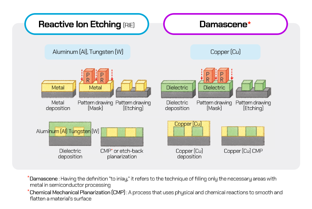
▲ Figure 5. Comparison of reactive ion etching (RIE) and the damascene process (Source: Hanol Publishing [Understanding Semiconductor Manufacturing Technology, p. 293])
The process of creating and connecting the wires unfolds very differently depending on the type of metal that’s intended to be deposited. If aluminum is going to be deposited, the wires can be made using the etching and deposition techniques that were explained in previous episodes. After applying a metal film over the entire surface of the wafer, photoresist needs to be applied on top before progressing to exposure. Then, after shaving off unwanted aluminum, various dielectrics—or insulating materials—are filled around the remaining aluminum.
In the case of copper (Cu), the order of metal and dielectric deposition is reversed. When copper is used to make wiring, the dielectric is deposited first and then etched afterwards using photolithography. A copper seed layer is then created, and the copper is filled in between the dielectric before the remaining copper is grinded away.
As a matter of fact, the order in which metal and dielectric deposition is carried out is significant. As explained earlier, copper requires the application of a seed layer which, in turn, requires a new deposition process. Moreover, a technique not used for aluminum called electroplating* also needs to be applied. In order to overcome the limitations of aluminum, it was necessary to not only apply copper as a new material in the semiconductor process but also develop various processes to enable its use. For a long time, it has been widely known that copper has better electrical properties than aluminum. However, for semiconductor companies, the manufacturing process also needed to evolve to allow copper to be applied to transistors that are produced on a larger scale at lower costs. Looking at metal wiring, it is thicker towards the top layers of the device. Although it is advantageous to place semiconductor devices that need to send and receive a lot of data frequently close to each other, devices that do not send and receive data back-and-forth as much can be connected over longer distances. These devices are connected by thicker metal wiring at the top.
* Electroplating: The process of coating metal from one side to another side using the principle of electrolysis.
This thick metal wiring on the upper parts does not require complex techniques to be created. Just as aluminum was used to create a bottom layer wiring of a certain thickness in the past, an aluminum wiring with the same thickness can be made on the upper part. So, the application of the top wiring layer does not have to involve advanced technology but can use processes that have been frequently used before. This not only cuts costs for the semiconductor company but also saves time as there is no need to learn and use a new process.
Combining Technologies to Achieve Progress
These technologies mentioned above do not exist in isolation but are combined in various ways by semiconductor manufacturing companies that produce semiconductors based on their strategies. Unlike memory chip makers like SK hynix, companies that manufacture logic semiconductors* need to be able to fully control the current in their transistors. To achieve this, they need to widen the area by introducing a three-dimensional structure such as a FinFET and make the channel where the current passes into a three-dimensional shape. It can be presumed that it is much more difficult to form contacts on a transistor with this structure compared to flat transistors used in DRAMs and other products. Looking at the left side of Figure 6, it is easy to bring the contact and the channel where the current flows close together. In contrast, the right side shows it is difficult to make a contact that is close to the channel.
* Logic semiconductor: A semiconductor with operational purposes such as a CPU or GPU.
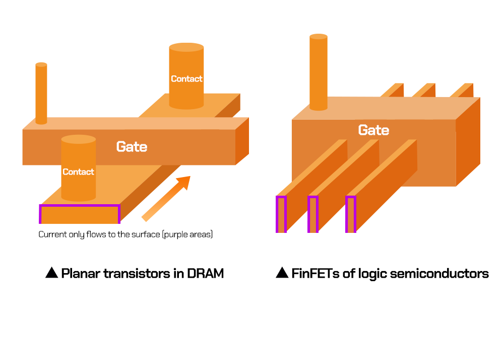
▲ Figure 6. Diagrams showing it is more difficult to form contacts in FinFETs of logic semiconductors (right) than planar transistors in DRAM (left)
As miniaturization progresses, these challenges are bound to continue. Memory companies like SK hynix do not face issues concerning the operation speed of the circuit but, instead, struggle maintaining charge capacity when stacking capacitors up high. The important thing to note is that the challenges of miniaturization, as well as metallization, will vary depending on the business environment of each company.
Semiconductor Manufacturing as a Collective Effort
Semiconductor manufacturing involves tens of thousands of workers while a single wafer must go through hundreds of steps to become a finished product. Therefore, those involved in each process contribute to less than 1% of the final product, but the semiconductor will not function if any one of these processes fail. Accordingly, the work that goes on in a semiconductor company is not completely independent; the work of one person influences the work of another, creating a big synergy effect.
One of the goals of this article is to help readers understand the technologies behind the processes. Nevertheless, a more important goal is to understand the relationship between the technologies. The material used in the deposition process affects subsequent processes that use heat and, also, the etching process. When etching is proceeded extensively, problems can occur for the entire product if the following deposition process does not have good gap-fill properties. If there are not enough steppers to draw fine patterns, a process involving additional hard mask deposition and etching, which is called multi-patterning* , is required.
* Multi-patterning: A technique that uses steppers multiple times to draw very fine patterns on a wafer.
As evident from the explanations above, the semiconductor industry does not only rely on high-tech processes but also trust. It is a sector that requires good communication skills, honest work, and creativity in coming up with new ideas. The development of semiconductor technology is a continuation of identifying problems by honestly sharing various challenges that arise when developing a new micro-process. Afterwards, the problem needs to be solved with the creativity of the organization which holds the solution. As seen in the photolithography process, a new problem caused by an immersion stepper was solved by using a photoresist instead of a stepper.
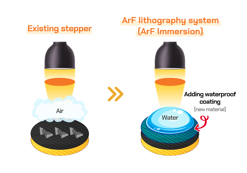
▲ Figure 7. Example of a photoresist solving an issue with a stepper
It is the hope that readers, especially those who desire to join the semiconductor sector, understand these aspects of the industry. Understanding these technologies can go a long way in assisting the development of careers while helping to create a virtuous cycle of relationships with many related organizations, which can eventually lead to creating the world’s best semiconductors.
Currently, semiconductor technology is facing major challenges in miniaturization. The voices of the people who use semiconductors need to be heard even more going forward. Likewise, the abilities of those who will communicate and develop technology within semiconductor companies will prove to be even more valuable in the future.