

Over the last few years, semiconductor memory has become more important and more in demand. That’s because it plays a significant role in development of the technologies behind the Fourth Industrial Revolution – such as big data, artificial intelligence (AI), the Internet of Things (IoT), smart factories and autonomous vehicles, among others. And while the forecasts suggest even more growth in the future, there’s also a push for new innovative technologies that go beyond what’s capable now. That will require creative thinking around both development and mass production of semiconductor memory.
For generations, technology has evolved to get us where we are today. The transistor, whose name derived from the transfer resistor, was invented after a long period of technological development. In 1951, the junction-gate field-effect transistor (JFET)1 was invented and in 1958, the resistor, capacitor2 and transistors were put into a circuit on a silicon semiconductor, marking the birth of the electronic circuit. Semiconductor technology advanced in earnest in the 1960s with the practical use of integrated circuits (ICs)3 , resulting in a new era of technology. After that came the metal–oxide–semiconductor field-effect transistor (MOSFET)4 invented by Dawon Kahng and Mohamed Atalla and complementary metal-oxide-semiconductor (CMOS)5 . Moreover, the integrated circuit made CMOS smaller, lighter and more sophisticated – and that allowed a single chip to hold more devices and perform better.
In 1965, Gordon Earle Moore introduced Moore’s Law6 , which focused on the development speed of microchip technology based on an observation that the amount of data that can be stored in a microchip doubles every 18 months. This law has had the effect on doubling the processing speed of computers and the amount of memory, and relatively reducing its costs. Most of the companies failed to follow Moore’s Law due to economic reasons, as more transistors had to be placed into a smaller space to enhance the performance of silicon chips as well as the heat dissipation challenge. Accordingly, it has been dismissed.

Figure 1. Moore’s Law
Throughout its history, the semiconductor industry has strived to minimize patterns. Inevitably, the result is greater process complexity and more limitations, which in turn leads to longer development times for new products and slower growth.
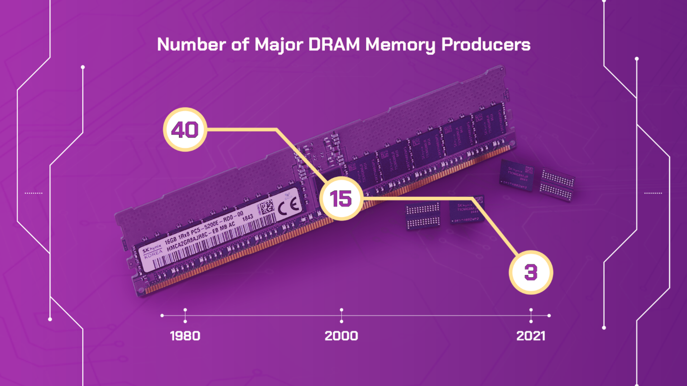
Figure 2. Number of Major DRAM Producers
(*Aggregated, these figures may differ from actual figures.)
It appears that the process of scaling down is faced with not only physical but also cost limitations. The overall numbers of both processes and extreme ultraviolet (EUV)-applied layers are increasing. Dynamic random-access memory (DRAM)7 is already reaching its limits to scale down. 3D NAND is continuing to grow density by increasing stacks without changing its design rule – and this also will reach its limits.
New technologies such as EUV8 are adopted to overcome technological limitations and materials are being developed to allow more scaling-down. The adoption of the EUV process reduced double patterning technology (DPT) processes. However, both the EUV and DPT9 technologies are applied when developing new products, which means that technological limitations and costs are growing.
While DRAM and NAND have been scaling down and advancing, both will be faced with limitations related to physical scaling. More technologies will be introduced to solve this problem but there will also be a need for new memory technologies to meet market demands.
Meanwhile, wafer size has been diversifying from 4-inch to 5-, 6-, 8- and 12-inch to produce more semiconductor products from one wafer, securing production competitiveness while also boosting bit growth. In this fourth Industrial Revolution, high-performance data processing is key, which means that semiconductors will require ultra-high performance and ultra-low power. The demand to process better quality data – and more of it – is surging, and that means that the entire industry, from production equipment to parts and materials to the technological innovation must also continue to advance to compete in a demanding, fast-growing market.
It’s important to remember that the semiconductor industry is really an equipment industry, which means there’s a need to make large-scale investments in facilities, which is also challenging because the industry is also highly sensitive to changes in supply and demand. Yet, the industry can be characterized by short lifecycles of products, rapid price changes caused by different market conditions, and high demand for more meticulous production processes.
Beyond the challenges of today come the preparation for the next generation of industry leaders who can drive semiconductor technology in the right direction as demands evolve. To get there, the industry will need to nurture people with institutional knowledge and groom a next generation that can foster innovation.
The industry is comprised of a range of fields that require deep understanding, which means that semiconductor companies need to proactively nurture talent for mid- and long-term periods, which involves the difficult task of cultivating expertise while simultaneously producing new experts. People study and learn in school, but they also grow by performing tasks themselves. That means that senior-level team members not only must do the work of today but also must mentor their junior-level colleagues. Training too many junior-level people over short periods of time can not only compromise the work of senior-level employees but also hinder the growth of junior-level colleagues, too.
The semiconductor industry requires competent experts in both development and mass production. Engineers specializing in design, device, process, and equipment must work together to develop and manufacture new products. Technological capacity in production equipment is especially vital to producing high quality products and high yield.
In the past, theory-based education was provided to foster technological capacity with a minimal number of trainees at equipment manufacturing facilities. But that creates another set of challenges. On-site training with expensive equipment that is used in real-world production creates potential for unexpected damage or increased maintenance time – which is time that the equipment would be out of use. While an outage could have a negative impact on productivity and overall efficiency, trainees still must learn how to operate the equipment and practice on-site to enhance their capabilities.
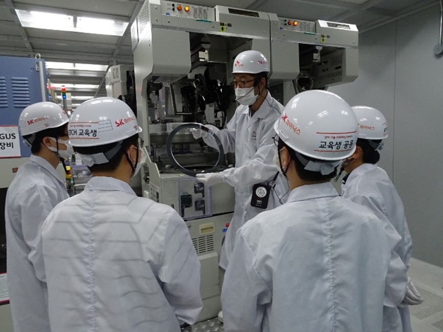
The instructor is explaining about oxide etching equipment
Trainees must be able to operate equipment themselves and practice on-site to enhance their practical capacity in equipment and technology. The aforementioned environment does not allow this. The best alternative is to establish infrastructure that enables hands-on training and learning. SK hynix has established and been improving internal infrastructure in 2017 to provide on-site training and learning on equipment. Our Equipment and Technology Training Center offers education on equipment and basic technology.
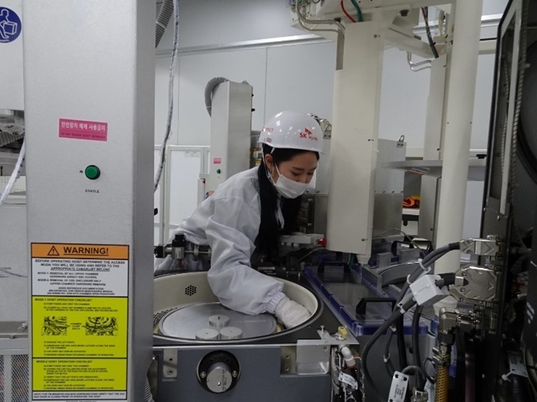
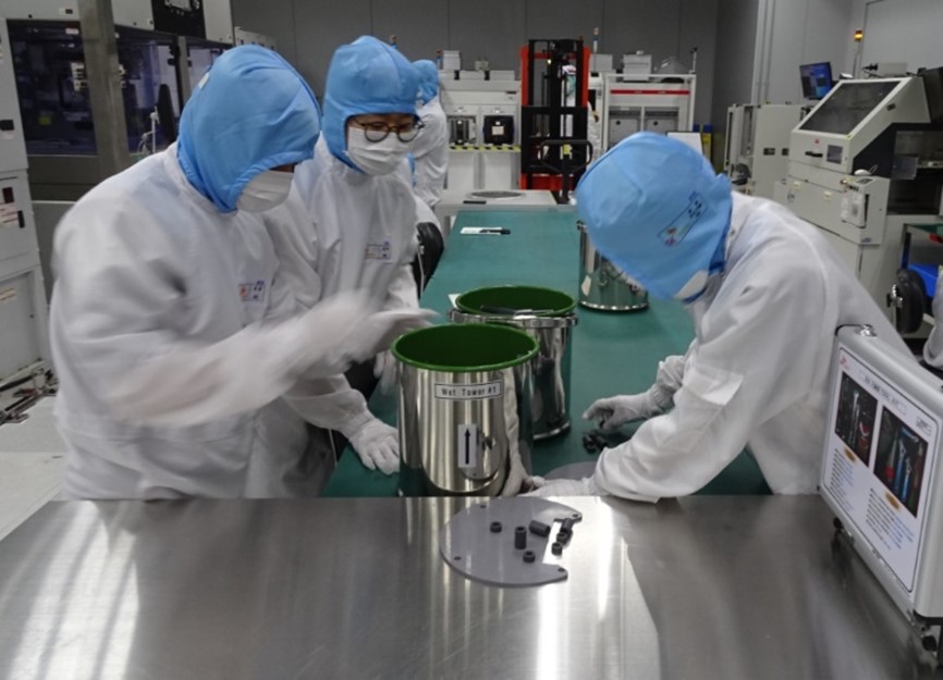
Trainees are practicing with poly etching equipment
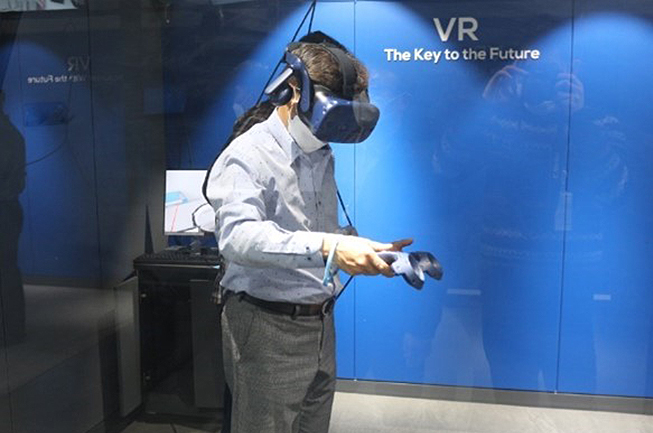
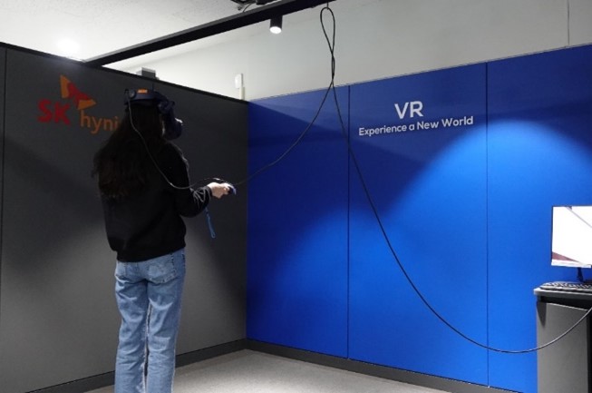
First, equipment training consists of hands-on equipment operation and educational VR content. Equipment training provides equipment for all areas and hands-on training to help trainees enhance their equipment capacity. However, not all equipment models can be housed, which also means that training on them cannot be provided. Consequently, training on a number of models is offered with VR content. We also offer tailored VR content training and practice on equipment for each trainee based on their capabilities. In particular, we are currently developing VR content to enhance educational capacity for newer equipment models and boost cost efficiency. Once VR content is fully developed, introductory and intermediate equipment training courses, introductory and intermediate VR education will be provided to complete our infrastructure for equipment and technology training.
Second, we have prepared and been offering training on basic technologies that constitute equipment and systems. There are nine courses on basic technologies (pump, chiller, ESC, MFC, sensor, RF generator, robot and gauge scrubber) that contribute to the capacity building of trainees. The program will be offered in our Cheongju Campus starting in January 2022.
Trainees participate in training on scrubber technology
The Equipment and Technology Training Center continues to establish training and theory-based courses to boost the equipment and technology capacity of trainees.
The SK hynix Equipment and Technology Training Center for manufacturing and technology employees was successfully established, thanks to executives as well as the early members who set up the center, trainers and staff who continue to improve our environment for education. Further development in semiconductor technologies will allow us to house more newer models in the future. With this in mind, the center continues to evolve and support the capacity building of all of its members.

An instructor is teaching a trainee on thin film CVD equipment
The semiconductor industry requires integrity, patience, collaboration and teamwork, especially because new product development and production will be challenging in the future. It needs integrity because success is tied directly to effort, just like the farming industry. Patience is required because engineers must have the grit to solve problems. Lastly, just like an orchestra, the industry requires teamwork and collaboration. If one player in an orchestra makes a mistake, the sound of the music changes. The same applies with the semiconductor industry. One error in any of the processes means the product has failed. The formula for semiconductor production technologies is 1000-1=0, rather than 1000-1≠999.
As such, only thoroughly trained experts can work in the industry. But at the same time, the industry offers vast number of opportunities, where these opportunities help the industry to lead change in the world. I hope those of you working in semiconductor material, part and equipment industries, and younger juniors who aspire to become the best semiconductor experts in the world, continue to aim for your dreams.
1Junction field effect transistor (JFET): A semiconductor device that involves carriers (electrons or positive holes) of only one polarity in internal electrical conduction within a semiconductor; also known as a unipolar transistor.
2Capacitor: A device that stores data in DRAM.
3Integrated Circuit (IC): A circuit consisting of only semiconductors and originally created with sophisticated semiconductor processing technology. Individual transistors, diodes, resistors and capacitors are integrated on a thin silicon wafer, which are then mutually connected through electrical circuits. Its volume is minimized, and it can be further divided into different types such as SSI, MSI, LSI, VLSI and ULSI depending on its level of integration.
4Metal Oxide Semiconductor FET (MOSFET): A field-effect transistor with a metal gate on a thin oxide layer on the silicon. MOSFET is the most typical insulated gate FET whose insulating film is made of an oxide layer. Consisting of a metal, an oxide and a semiconductor, MOSFET controls the electric current between the drain and source terminals using gate voltage.
5Complementary Metal Oxide Silicon (CMOS): A complementary logic circuit consisting of pairs of n-channel and p-channel MOSFETs. CMOS devices consume low power. CMOS is used in DRAM and CPU as it is capable of ultra-large-scale integration although its processors are complex.
6Moore’s Law: A law about the speed of the development of microchip technology. The law observes that the amount of data that can be stored in a microchip doubles every 18 months. The law was first introduced by Gordon Moore in 1965 as he forecast the capacity of microchips will double every year. The time frame was revised to 24 months in 1975, then again to 18 months. As a result of Moore’s Law, the processing speed and memory of computers doubled with relatively lower costs. The law led to a digital revolution where American computer companies in the late 1990s heavily invested in ICT.
7Dynamic Random Access Memory (DRAM): RAM is computer memory that can be read and changed and used to store data temporarily. DRAM is a type of RAM that needs to be refreshed regularly as stored data leak away as time passes. DRAM is used for temporary large-scale data storage.
8EUV: Extreme Ultra-Violet.
9Double Patterning Technology.
[Glossary]
1. Information and Communications Technologies (ICT): Technologies related to information and communication. The term information technology (IT) is more commonly used in Korea and other Asian countries, although the term ICT is more widely used globally.
2. DT (Digital Transformation): A phenomenon that occurs when an organization adopts a new innovative business method to keep up with technological development. The term refers to a cultural change where digital tools are used to bring about fundamental changes, or to improve existing methods or replace them with something new.
3. Semiconductor: A material in between the conductor and insulator. Although a semiconductor is similar to the insulator when it is in its pure state, adding impurities can increase its electrical conductivity. The range of semiconductor resistivity is typically between 10-3 and 10-1Ωcm in room temperature but may vary.
4. Transistor (Tr): A semiconductor device that controls an electric current or a voltage flow to amplify it or work as a switch. Composed of an emitter, a base and a collector, a transistor can control the electric current or voltage between two of its parts caused by the other part’s electric current or voltage.
5. Diode: There are many types of diodes. A rectifier diode allows an electric current to flow in only one direction and not the opposite. A switching diode is used in logic circuits, while a voltage diode is used in constant voltage circuits. A light-emitting diode emits light, while a variable capacitance diode changes the capacitance depending on the voltage.
6. Silicon Transistor: A transistor made with a silicon base. Silicon transistors have better withstand voltage and current capacity than germanium transistors and are more widely used.
7. Planar Technology: A semiconductor device technology that uses selective diffusion, ion implantation and photo etching to form devices on the same plane of substrate crystals, making a plane even and flat.
8. NAND Flash: NAND flash is non-volatile memory that does not require power to retain data within a chip. Its main structural difference from DRAM is that it is made of two types of gates.
9. Phase Change Random Access Memory (PCRAM): Next-generation non-volatile memory that detects changes in the state of materials to store data.
10. Resistance Random Access Memory (ReRAM): Next-generation non-volatile memory that works by changing the resistance depending on electrical signals.
11. Bit Growth: Refers to the overall growth rates of semiconductor memory. A bit is used as a unit to calculate memory capacity. The concept was introduced to prevent distortion when calculating growth rates using the amount of memory produced.


