Although technological advancements in the semiconductor industry are reaching their limits and development costs are continuing to rise, the market continues to demand ever-improving technologies. To bridge this gap in technological progress and meet the market’s needs, one solution has emerged for semiconductor companies—advanced packaging technology. And at the heart of this highly complex technology is interconnection technology.
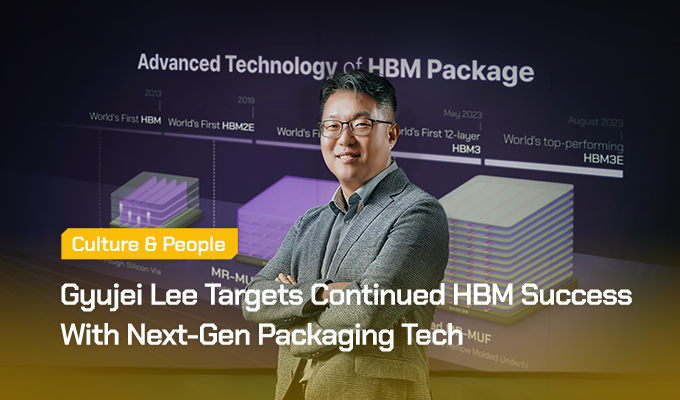
In this EE Times article, Ki-ill Moon, the head of PKG Technology Development at SK hynix, covers the evolution of packaging technology and highlights some of the company’s recent efforts and accomplishments in helping to advance the field.
As the speed, density, and functions of a semiconductor product vary depending on how the interconnection is made, interconnection methods during the packaging process are constantly changing and developing as mentioned by Moon in his previous article.
More specifically, the following four types of interconnection techniques have gradually developed over time to eventually provide more efficient and high-quality packaging techniques: wire bonding, flip chip bonding, through-silicon via* (TSV) bonding, and hybrid bonding with chiplets.
* Through-silicon via (TSV): A type of vertical interconnect access (via) that completely passes through a silicon die or wafer to enable the stacking of silicon dice.
With traditional wire bonding technology advancing all the way to the more recent hybrid bonding with chiplets, unprecedented achievements have been made through improvements in the package’s cost-effectiveness, operating speed, flexibility of chip design, thermal dissipation, and size reduction.
Following such developments, SK hynix developed the world’s first-ever 12-layer HBM3 in April 2023. Furthermore, the company plans to use the most high-powered packaging solution to develop hybrid bonding so it can be applied to its future HBM products such as the 16-layer HBM.
To find out more about the technologies that will help SK hynix elevate its packaging technologies and platform solutions to unprecedented levels, read the full EE Times article here: The Role of Interconnection in the Evolution of Advanced Packaging Technology