Visual Evolution – from the Cambrian Era to Today
Close your eyes and imagine a world without eyesight.
Millions of years ago, that was the way of life on Earth. It was nearly 540 million years ago that animals first developed the ability to see – transforming everything about the ways in which they could avoid enemies, secure food, and evolve into various species.1 It led to a geological event known as the Cambrian explosion, where the number of animal groups exploded from three to 38.
A similar visual innovation took place much more recently with the proliferation of smartphones in the late 2000s. Suddenly, people around the world were equipped with high-performance cameras that could fit into their pocket or the palm of their hand. Photography was no longer restricted to photographers and the easy transfer of visual information became widely available.
This year, with the outbreak of COVID-19, the transition to the contactless digital era accelerated once again as video conferencing and online classes became a part of our daily lives.
1Andrew Parker, “In the Blink of an Eye: How Vision Sparked the Big Bang of Evolution”, (2003) (URL)
“Retina of Camera” CIS Technology Development, the Heyday of Smartphone Cameras
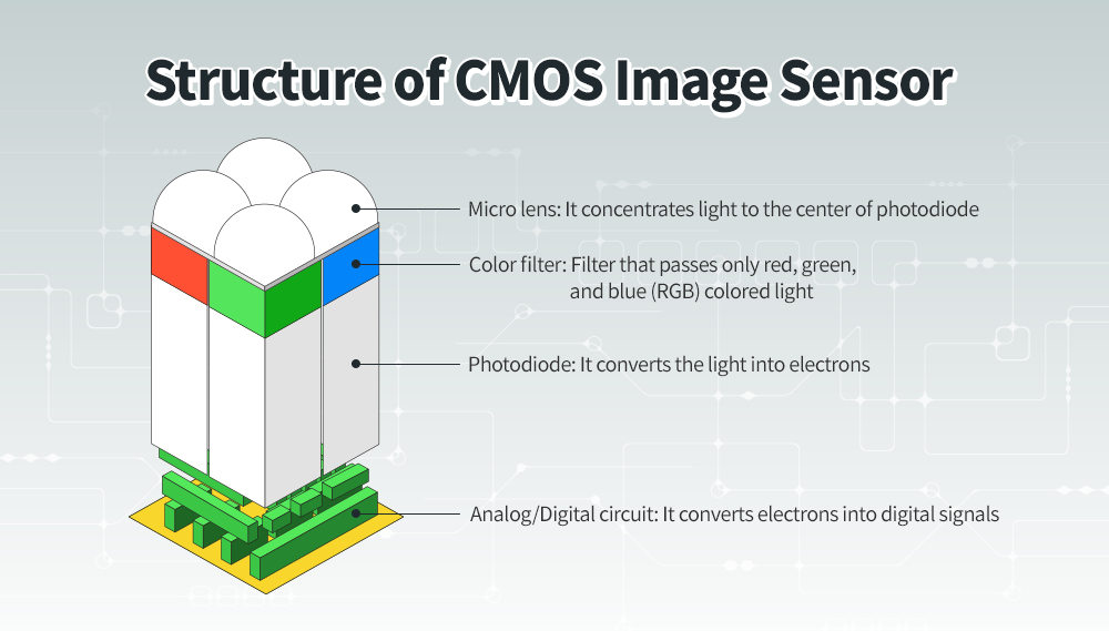
Figure 1. Structure of CMOS Image Sensor
A camera is designed much like the human eye.
A smartphone camera is composed of various parts such as a lens, infrared cut-off filter2, auto focusing actuator,3 and CMOS image sensor (CIS).4 Among them, CIS is a key component that acts as a retina of the human eye. As shown in Figure 1, it is composed of a photodiode that converts light into electrons, a color filter where only the light of a specific wavelength can pass through, an analog/digital circuit that converts electrons into digital signals, and an image signal processor (ISP) responsible for correction and image processing.
Since the resolution, sensitivity, and signal-to-noise ratio (SNR)5 are determined by the CIS performance, it can be said that the image quality of the smartphone camera is determined by the CIS. Today, the CIS image quality of smartphone cameras has surpassed the level of compact cameras, and the gap from DSLRs is continually being narrowed.6
In terms of performance, CIS has developed in the direction of reinforcing the number of pixels and its functions. Since more detailed and clearer image quality can be obtained with the increase in the number of pixels, the competition for the higher number of pixels started from the early stage of smartphone cameras. In addition, with innovations in semiconductor micro-processing such as back side illumination (BSI)7 and deep trench isolation (DTI)8, more pixels are integrated in the same size of area, making it possible to easily capture images of tens of millions of pixels even in a general smartphone.
2Infrared cut-off filter: A device that only passes the visible light and blocks the infrared wavelength
3Auto focusing actuator: A lens driving device for autofocusing, implemented with a small motor
4CIS: A device that can detect light and convert it into an electrical signal with a structure of ‘Complementary Metal Oxide Semiconductor (CMOS)’ composed of different MOS integrated circuits.
Acts as an electronic film in fliming electronic devices such as smartphones and cameras with high speed and low power consumption.
5SNR (Signal-to-Noise Ration): Defined as 20 log (signal/noise)
6David Cardinal, “Smartphones vs Cameras: Closing the gap on image quality”, DXO Mark. (2020) (URL)
7BSI (Back Side Illumination): A technology that increases the amount of light received on a photodiode by accepting light from the rear of the sensor. When light enters from the front of the sensor, light loss occurs due to scattering by metal wiring.
8DTI (Deep Trench Isolation): Process technology to make barriers between physical pixels between adjacent photodiodes inside silicon to prevent signal interference between pixels.
The Latest Technology Trend in CIS is about Function, not Pixel
Nevertheless, this trend for high pixels in CIS is expected to face technical difficulties soon, and the innovation for a high level of functions centered on the ISP will be in full swing.
This is due to the limits of miniaturization of CIS pixels due to the diffraction limit9. CIS is a complex component that combines optical technologies such as micro lenses and semiconductor technologies such as devices and circuits. It is possible to reduce the critical dimension of electric circuits to several nanometers with the current semiconductor technology; however, since the light reception amount decreases as the pixel size decreases, the sensitivity and the signal level is reduced, resulting in the decline in SNR and the image quality degradation.
9Diffraction limit: A limit point in which the distance between two objects is too close, making it difficult to distinguish with an optical lens.

Figure 2. Airy disk diffraction image
The optical system of the camera also has a physical limit where the performance is limited by the diffraction effect,10 and even if one point light source11 is taken, the image formed on the CIS through the lens is spread out, as seen in Figure 2. This is called an airy disk12; given the wavelength (λ), focal length (f), and lens diameter (d), the distance (x) that can separate the two points is determined by the following formula:

10Diffraction effect: A phenomenon in which light proceeds in a curved path rather than a straight path when it encounters an obstacle.
11Point light source: A light source that is small enough to be considered as a dot.
12Airy disk: A phenomenon that the image is spread out when one point light source is condensed on the CIS through the lens.
For example, for a 400nm blue point light source, even if a high-performance lens with an F (=f/d) number of 1.4 is used, the distance that can separate the two points is 0.68μm. In other words, to distinguish the two blue point light sources, the distance should be at least 0.68μm. Therefore, even if the size of CIS pixels is made smaller than this, it is difficult to expect substantial improvement in resolution. Since the size of the commercially available CIS pixel has already reached 0.7 to 0.8μm, it is necessary to develop a new optical technology to reduce the F number or a new application that can merge several fine pixels.
Another reason for this innovation is the emergence of stack sensor technology. Since the conventional sensor has a structure where pixels and circuits are implemented on the same substrate, it was essential to reduce the light-free area for the CIS size reduction. Therefore, only essential functions of analog/digital circuits were implemented and adding circuits for additional functions was very limited.

Figure 3. Left: Conventional sensor structure / Right: Stack sensor structure (right)
On the contrary, the stack sensor has a structure where pixels and circuits are implemented on separate substrates as shown in Figure 3, and then the two substrates are connected electrically by Through Silicon Via (TSV)13 or hybrid bonding technology.14 Since pixels and circuits are stacked together, the circuits on the lower substrate can be used as much as the area occupied by the pixels on the upper substrate, leading that area free to use.
13TSV (Through Sillicon Via): An interconnecting technology that delivers electric signals through column-shaped paths that penetrate the entire silicon wafer thickness.
14Hybrid bonding technology: A process technology that bonds metal electrodes of two wafers together and connects them, instead of an electrode penetrating through a silicon wafer. It can reduce size while increasing performance.
For example, a 48 megapixel (8,000 x 6,000) sensor implemented with 1μm occupies an area of 48mm2 or more on the upper substrate. If this size of area on the lower substrate can be used for the implementation of digital logic, it is possible to utilize a large space, enough to integrate a large number of high-performance microprocessors.15
In addition, the stack sensor has the advantage that an independent process can be applied to the pixels on the upper substrate and the circuits on the lower substrate. If an advanced logic process16 is applied to the lower substrate for circuits, even a complicated ISP algorithm can be implemented with low power, high density digital circuits. In other words, while the ISP of the conventional sensor only supported simple functions such as lens correction and defect correction due to the limitation of the circuit area, the ISP of the stack sensor can implement innovative algorithms such as image processing, computer vision, and artificial intelligence (AI) by using an advanced logic process.
15Microprocessor: A device that integrates the control functions of the processing unit and central processing unit into one chip
16Logic process: Semiconductor process that manufactures digital devices to process logical operations such as AND, OR, NOT
SK hynix’s CIS with Various Functions
Currently, SK hynix’s CIS has built-in image processing functions such as phase detection auto focus (PDAF), Quad pixel processing, and high dynamic range (HDR) processing, and new functions are constantly being added to it.

Figure 4. Left: Half Shield PDAF structure / Right: Paired PDAF structure
PDAF is a function that applies the principle that human’s both eyes use to predict the distance to a subject. That is, for some pixels of the CIS, this method generates a phase difference17 by covering the left and right, as shown in the left side of Figure 4, or by placing the left and right pixels under one large micro lens as shown in the right side of Figure 4. Through this method, the ISP algorithm calculates the phase difference from the left and right images and converts it into a distance to the subject to focus quickly and accurately.
17Phase difference : The phase difference between two vibrations (wavelengths). The phase refers to the relative position of the vibration(wavelength) at a certain point.

Figure 5. Left: Output of a conventional sensor / Right: Output of a Quad sensor
The Quad sensor has the function of placing four color filters of the same color adjacent to each other and processing them together. In dark places, four pixels are combined and processed to receive more light and in bright places, the individual pixels are separately processed by the ISP algorithm to improve resolution. Figure 5 shows two images taken with SK hynix’s 48 megapixel Quad sensor and a conventional sensor, respectively. This shows that it is possible to obtain a bright image without noise even in a dark place when using a Quad sensor, compared to when using a conventional sensor.
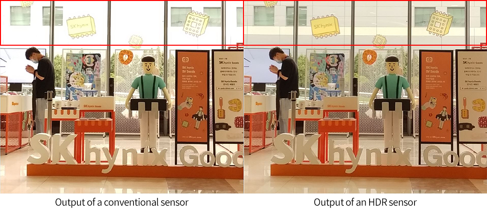
Figure 6. Left: Output of a conventional sensor / Right: Output of an HDR sensor
The HDR sensor supports a function that makes a clear contrast between the bright and dark parts of an image by synthesizing multiple pixels with different sensitivity and exposure time. In particular, with the SK hynix’s CIS, image processing is performed by a built-in ISP, resulting in real-time processing and clear image quality even with a moving object. Figure 6 shows the output images with and without HDR application to the SK hynix’s CIS. Compared to the image where HDR is not used, the image using HDR restores the background clearly while maintaining the same brightness of the whole image.
Currently, SK hynix’s CIS, mainly the Black Pearl product line, is widely used in smartphone cameras and the application field is expected to expand to various fields such as bio, security, and autonomous vehicles.

Figure 7. Camera mounting location in self-driving car
In particular, autonomous vehicles use at least ten cameras to detect their surroundings.18 To improve accuracy, various requirements such as high resolution support for distinguishing distance objects, HDR support for recognizing objects even in dark environments, and pre-processing of the ISP to reduce the computational amount of the processor must be satisfied.
In the security field, a function to compress and encrypt image signals in the CIS built-in ISP and to transmit them to an external processor is required. If the unencrypted image signal is transmitted to the outside as it is, the possibility of security vulnerability and information leakage increases. For this reason, the encryption function inside the CIS is essential.
18Peter Brown, “Breaking Down the Sensors Used in Self-Driving Cars”, Electronics 360. (2018) (URL)
The future of CIS: Information Sensor that supports advanced functions
In the future, CIS is expected to evolve into an information sensor that supports advanced additional functions, without being limited to image quality improvement.19 SK hynix’s stack sensor is already capable of embedding a simple AI hardware engine inside the ISP on the lower substrate, based on the advanced semiconductor process. Based on this, SK hynix is currently developing new machine learning-based technologies such as super resolution, color restoration, face recognition, and object recognition.
19Sungjoo Hong, “Smart Cloud and Information Sensor”, Smart Cloud Show. (2018) (URL)
Since it is possible to extract and classify various features from input images when using machine learning-based ISP technology, CIS will become a key component of information sensors that collect various information such as image information, location information, distance information, and biometric information.
In particular, to utilize CIS as an information sensor, it is necessary to take a new approach from a different perspective. This is because the quality goal of CIS is now “achieving the image quality optimized for machine algorithms”, while the goal was previously “achieving the image quality optimized for human eyes” so far.
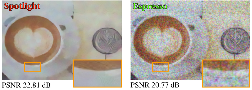
Figure 7. Left: Less noise but misrecognized as a spotlight
Right: More noise but accurately recognized as an espresso
According to the results of a research of Stanford University, even if a good-looking image to the human eye is created through complex image processing, it does not always mean that this image produces excellent results when computer vision algorithms are applied to it. For example, when an object recognition algorithm is applied to the coffee cup image in Figure 7, the image on the left with less noise is incorrectly recognized as a spotlight, but the image on the right with much more noise is accurately recognized as an espresso. This shows that the key function for the future CIS is to provide image quality optimized for the computer algorithm to be used.20
20Diamond, V. Sitzmann, S. Boyd, G. Wetzstein, F. Heide ‘Dirty Pixels: Optimizing Image Classification Architectures for Raw Sensor Data’, arXiv preprint arXiv:1701.06487.
As explained in this article, SK hynix is increasing the level of integration of the CIS pixels through the continuous development of device and process technologies and supporting various application fields through the ISP technology development. Especially, to pioneer new technology fields, it has established and is operating overseas research institutes in Japan and the United States, and various researches are actively being conducted with domestic and foreign universities through the academic-industrial collaboration. In the future, SK hynix’s CIS is expected to be utilized in various application fields including smartphone cameras to contribute to the creation of economic and social value and to grow as a key component of information sensors in the future.

ByTae-hyun (Ted) Kim, Ph.D.
Head of CIS ISP at SK hynix Inc.