With the opening of the 4th industrial revolution era and the spread of high technologies such as artificial intelligence (AI), 5G, and autonomous driving, the demand for high-performance and ultra-small semiconductors is exploding. Accordingly, “packaging” technology, where semiconductors become solutions to have the best performance and create high added value, is now drawing great attention.
Along with this trend, SK hynix is also focusing on securing future competitiveness by paying attention to the packaging business through active investment and continuous technology development. This time, the newsroom team met with Seung Taek Yang, KI-ILL Moon, Jinwoo Park, and Ho-Young Son – Project Leader (PL) of the SK hynix’s PKG Development Division to hear about the present and the future of SK hynix’s packaging technology including conventional package, Through-Silicon Via (TSV), and Fan-Out Wafer-Level Package (FO-WLP).
Packaging Technology Determines Future Competitiveness as the Key to Increasing the Memory Product Value
After the front-end process where circuits are formed on a wafer, semiconductor chips go through the back-end process consisting of a packaging process and a test. Although a number of fine electric circuits are integrated on a chip, the chip itself cannot perform the role of a semiconductor. The packaging process serves to connect a chip electrically to the outside so that the chip can function properly and protect it from the external environment. Also, another role of packaging is to control heat generation to ensure efficient thermal emission by semiconductors.
With the advancement of semiconductor technology which makes semiconductor products faster and more functional, thermal problems are becoming more and more serious, resulting in the greater importance of the thermal dissipation of semiconductor packages. Also, even if the chip speed is high, as the electrical connection path to the system is made during the packaging process, packaging should also be implemented at a high speed to respond to the faster chip speed. For this reason, cutting-edge packaging technology for the high-density, high-speed, low-power, small-from-factor, and high-reliability semiconductor market is crucial.
▲ Seung Taek Yang PL
“Packaging technology is very important for high-performance devices to perform properly. For example, to transmit and receive a large amount of data at once, numerous electric paths connected to the outside should be formed, and what plays this role is the packaging process. Packaging technology stacks multiple chips to implement a capacity of four times, 16 times, or even more compared to the conventional chips, or combines several types of chips to create a system. In other words, depending on the packaging technology, the added value of a product can highly increase. Now, it is an era where chip technology alone cannot preoccupy the future market dominance without advances in packaging technology.”
SK hynix’s Packaging Technology, How Has It Developed?
As mentioned above, semiconductor packaging plays various roles including mechanical protection, electrical connection, mechanical connection, and thermal dissipation. In detail, during the packaging process, semiconductor chips are wrapped with a packaging material such as an Epoxy Molding Compound (EMC)* to protect them from external mechanical and chemical impacts. In addition, the packaging process physically or electrically connects the chips to a system to supply power to operate chips, ensures input and output of signals to perform desired functions, and allows dissipation of heat generated when semiconductor products are operated.
The methods of packaging semiconductors can be largely divided into two types. One is the conventional package, which is a traditional method of applying a packaging process to individual chips separated from wafers. The other is the Wafer-Level Package (WLP), where part or all of the process is carried out at the wafer stage and later cut into single pieces.
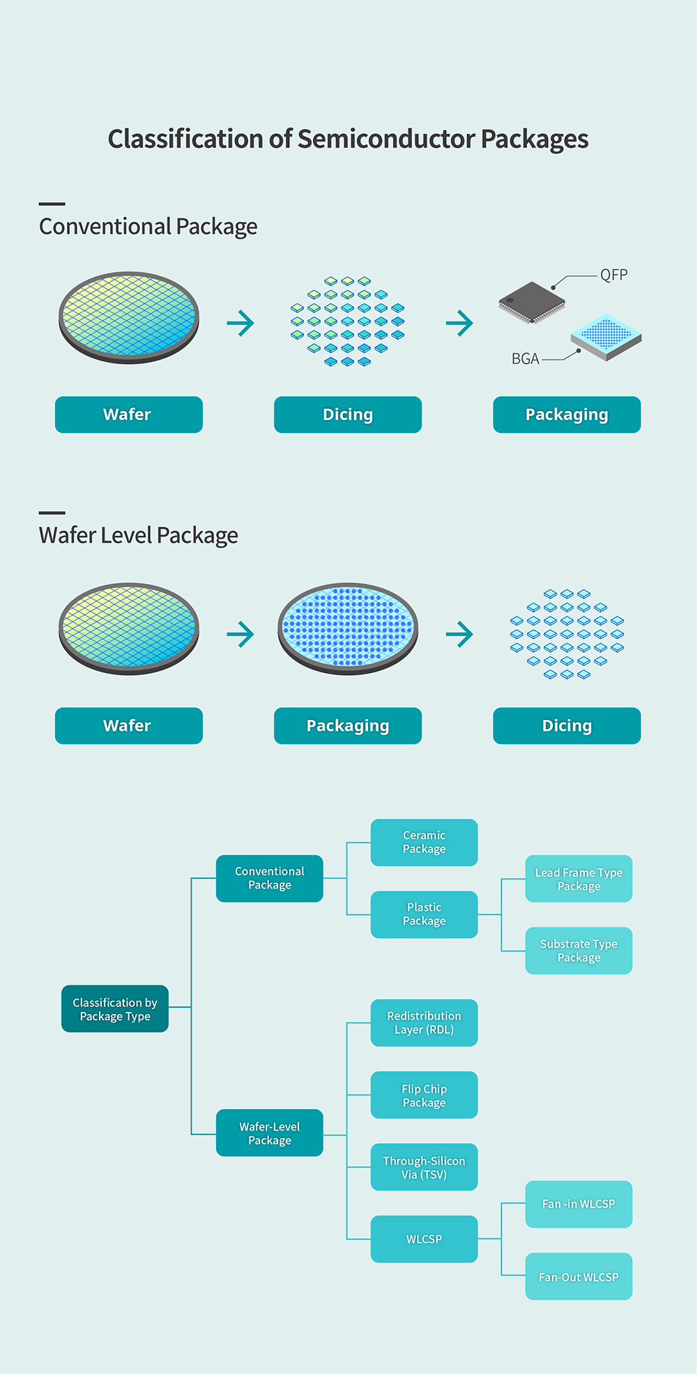
In the packaging field as well, SK hynix has continuously developed and created innovative products from the past to the present. The early packaging technology used in 1986, when DRAM development and production began in earnest, was the lead frame* method that connects chips and pads by using gold wires. Soon after, however, the lead frame structure faced its limit, with the improvement in the device performance. Accordingly, other structures such as the Fine-Pitch Ball Grid Array (FBGA)* based on a substrate are applied. This type of package is a conventional package, which is mainly applied to high-density NAND or mobile DRAM products since it can stack many chips in a package.
Since then, to meet the high-performance specifications required for memory products, the existing method of the conventional package has been developed and the new method of WLP has begun to be introduced, resulting in two paths of the development of the packaging technology. In particular, WLP technology is suitable for realizing high-performance products. Since packaging in the same size as the chip is possible when using this technology, it can minimize the size of finished semiconductor products. Also, saving cost is another advantage of this technology as it does not require materials such as substrates or wires.
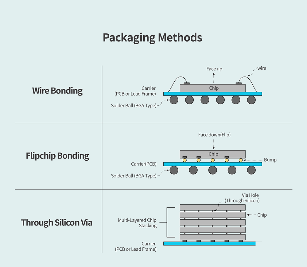
From 2007, SK hynix has introduced the flip chip* process, a technology that combines conventional packaging and WLP in graphics DRAM that requires high performance, while applying the Redistribution Layer (RDL)* process to the main memory. From 2007 to 2010, SK hynix revealed a series of memory modules to which the Wafer-Level Chip Scale Package (WLCSP)* was applied for the first time in the world. Based on this technology, the company applied the 3-Dimensional Stack (3DS)* and introduced a 128 GB DRAM module.
More recently, the WLP process is mainly used for products such as High Bandwidth Memory (HBM), which needs to satisfy the needs for high density and high performance, and Computing DRAM, which requires much more capacity than existing products.
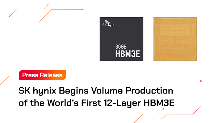
In 2013, SK hynix succeeded in developing and mass-producing HBM with TSV structure for the first time in the world and mass-produced 3DS products developed for High-Density products. In 2019, the company developed HBM2E and succeeded in mass-producing it just in 10 months, preoccupying a clear advantage in the HBM market and maintaining it until now.
Next-Generation Packaging Technology as a Growth Source of SK hynix
With the increase in the demand for high-performance and ultra-small semiconductors, packaging technology is emerging as a core technology for the next-generation semiconductors to enhance semiconductor performance and production efficiency. Accordingly, SK hynix is actively developing innovative technologies to raise the value of memory solutions by strengthening the packaging competitiveness in the fields of the conventional package, TSV, and FO-WLP.
> “Conventional Package” through a Total Solution of Materials, Processes, and Equipment
For a single package to implement High Density, the key is to stack chips as thin as possible, which requires high-level element technologies. In this regard, KI ILL Moon PL explained the SK hynix’s technology level by presenting an index of “chip stack count”.
▲ KI ILL Moon PL
“SK hynix’s packaging technology is the highest level in the industry. In the case of mobile DRAM, 16 GB is achieved by integrating 16 units of 8 Gb memory in one package. In the case of NAND, a product in which 16 layers are stacked in a package is mass-produced. In addition, SK hynix is in the process of securing element technology to apply 32-layer stacking technology to mass-produced products for the first time in the industry.”
What is the competitiveness unique to SK hynix, especially in the conventional package stage to survive in the increasingly fierce competition for miniaturization and stacking? Currently, SK hynix is preparing various solutions to maximize the performance required for each characteristic of memory products.
In computing and graphics memory, the power control function is crucial as well as high speed. To achieve this, SK hynix is preparing thermal dissipation solutions for easier power control. In terms of materials and structures, the company is developing various solutions including thermal dissipation EMC and Exposed Mold Package. Also, in the case of mobile memory where the speed determines its competitiveness, wire bonding technology is being developed to reduce signal delay or capacity.
In NAND, the complex solution of the combination of controller and DRAM determines the competitiveness. For this reason, SK hynix is developing element technologies in advance so that they can be used as needed to ensure a timely supply of various solutions to customers.
As the performance of electronic products evolves, the required level for semiconductors continues to increase as well. How can SK hynix overcome the limitations in the future? Moon PL said, “Every moment, we have been facing a limit and even now, we are facing one. However, we always have been overcoming the limit, like we are now.”
For instance, just a few years ago, it was considered impossible to reduce the chip thickness below 50 ㎛ to stack eight DRAMs. Now, however, it has become a very common technology. Moon PL said, “The reason we could overcome the limit at that time was the development of the equipment, processes, and materials that could handle thin dies. We will continue to take the lead in overcoming the limits in the future through various efforts such as boundless cooperation encompassing different functions of materials, processes, and equipment in the packaging field and seeking for a total solution.”
> “TSV” for Realizing High-Performance and High-Density Memory
To become a winner in the ultra-speed memory HBM market, a technology gap with competitors should be widened, going beyond the level of customer demand. To achieve this, the PKG Development Division developed an exclusive, specialized technology called Mass Reflow Molded Underfill (MR-MUF)* for the first time in the world and applied it to HBM products. Based on this technology, the thermal dissipation performance has been improved by more than 10℃ compared to competitors.
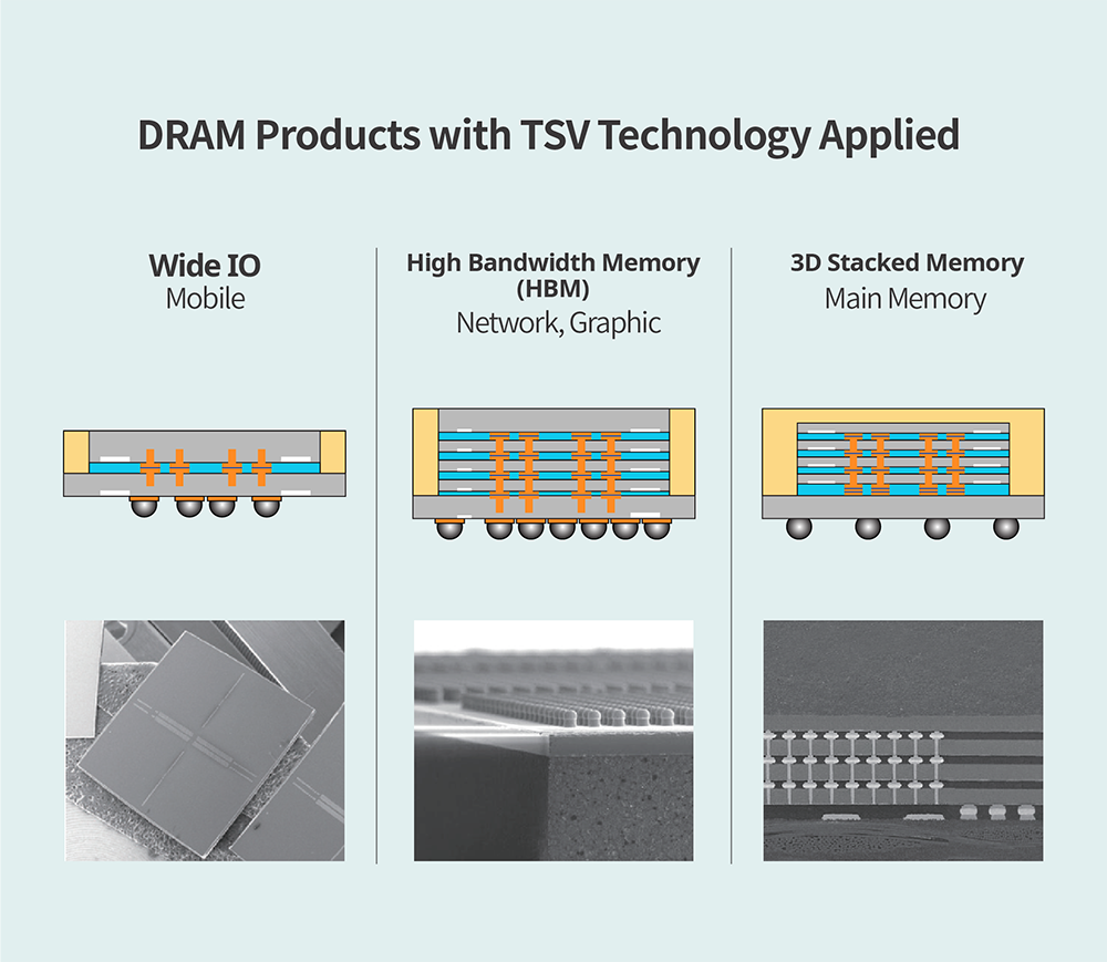
Meanwhile, TSV technology was the key to the innovative enhancement in the processing speed of HBM2E, “the world’s fastest DRAM”. SK hynix has implemented 16 GB, which is more than double compared to the previous generation by connecting eight 16 Gb DRAM chips vertically with the TSV technology. TSV is one of the WLP technologies that SK hynix is currently focusing on, and SK hynix has the highest level of TSV competitiveness in the industry.

▲ Jinwoo Park PL
“SK hynix has secured element technologies essential for stably handling thin wafers and stacking thin chips. We have developed the Advanced Mass Reflow method, which can stack 30㎛-thick chips in multiple layers as of today. Another competitiveness of SK hynix is the organizational power to ‘realize what we need to do’ rather than ‘realize what we can do’, based on the experience of succeeding in the HBM2E development. Our differentiated competitiveness is the process of collaborating between members and seeking a solution together even in difficult situations.”
In addition to the HBM2E, 3DS products are also one of the examples of innovation in TSV technology. Previously, the Mass Reflow (MR)* process commonly used in the flip chip method had been converted to the Thermal Compression (TC)* process for multi-layer stacking and miniaturization, but it has reached the limit of productivity. To overcome this, SK hynix applied the MR method to 3DS for the first time in the world, enabling stable production and quality control. This product is expected to be even more highly favored in the near future, since the DDR5 high-density market will be completely converted to 3DS.
SK hynix’s goal this year is to increase the TSV product line and secure profitability. To achieve this goal, company-wide efforts are being made.
Park PL said, “The core of the TSV technology is to implement stacking in a stable structure, quickly and cost-effectively. The TSV technology is applied only to HBM and 3DS products currently, but this can be extended and applied to mobile and NAND products, when high processing speed is needed. In preparation for this, we are working hard in collaboration with many other departments to proactively secure cost competitiveness.
> “FO-WLP”, a Packaging Technology of the Next Generation
In addition to the flagship packaging technology, SK hynix is focusing on the “Fan-Out Wafer-Level Package (FO-WLP)” as a growth source and a technology to contribute to profit generation in the future.
Wafer-Level Chip Scale Package (WLCSP) can be divided into Fan-In Wafer-Level Package (FI-WLP) and Fan-Out Wafer-Level Package (FO-WLP). Both technologies adopt a method of packaging by attaching solder balls (I/O terminals) directly onto the chip without a medium such as a substrate. As the length of wiring is reduced, the electrical characteristics are improved, and more chips can be stacked by reducing the package thickness.
Here, the “fan” refers to the chip size. When the chip size is the same as the package size and the solder balls for packages are implemented within the chip size, it is called “fan-in”. When the package size is larger than the chip size and the solder balls are implemented outside the chip as well, it is called “fan-out”.
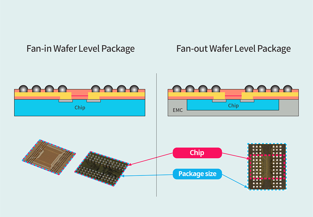
In the case of FI-WLP, where the chip size is just same as the package size, it has a disadvantage of having to establish a new package infrastructure when a new chip is developed, since a new chip requires a different package size even though it has the same function as the previous one. In addition, if the size of the package solder ball arrangement is larger than the chip size, the package cannot be made. It is also inefficient in that defective chips should be packaged as well, since the wafer is cut after the packaging process is completed. On the contrary, in the case of FO-WLP, there is no need to package defective chips because chips are cut first before the process. Since the package size can be adjusted, it is possible to use the existing package test infrastructure and it is easy to implement the desired package solder ball arrangement. Especially, it is advantageous in that different chips can be mounted in a single package as horizontal connection with heterogeneous chips is possible.
▲ Ho-Young Son PL
“FO-WLP is mainly used for packaging at least two heterogeneous devices such as packaging different System on a Chip (SoC) dies or packaging an SoC and a memory chip together. It is considered a next-generation packaging technology that will satisfy the demand for high-performance products. For this reason, many foundry companies are jumping into the back-end process technology development and expanding the market based on high technology and solid business models. SK hynix is also strengthening its investments in infrastructure related to FO-WLP technology, aiming for the company’s mid to long-term growth. Also, SK hynix is steadily preparing for the application of the FO-WLP technology for each memory application, as well as developing element technologies step by step to implement products.”
Currently, SK hynix is priorly reviewing adopting the FO-WLP to memory products. It is expected that it will significantly improve the package size and device characteristics by eliminating the need to use substrate while stacking multiple, identical chips. This will be also useful to implement a package structure that dramatically improves the performance limit of the current DRAM. Ultimately, it is expected to accelerate the development of direct packaging technology for heterogeneous devices such as memory and SoC and facilitate active participation in the semiconductor ecosystem environment.
Meanwhile, Son PL emphasized the necessity of understanding the memory system better than anything else. Based on the understanding, especially on the limitations of the current memory devices, it is important to find a solution through close cooperation between related departments to overcome such limitations, Son PL said.
In addition, he showed the determination to lead the semiconductor market in the new path based on the next-generation packaging technology.
He said, “HBM products were developed by SK hynix for the first time in the world eight years ago, and have been advanced through many trials and errors. Only recently, they have become technologically competitive and started to contribute to financial achievements. Looking back to this, you can see that it takes a long time for new technology to be adopted in the market and contribute to generating profits. This also means that if we do not prepare for the future from this moment, we will not be able to survive the rapidly changing semiconductor competition.”
Lastly, he expressed his confidence in SK hynix’s future, by saying, “We believe that we will be able to lead the market with competitive technologies if we continue to carefully prepare new technologies step by step without limiting ourselves. A number of members from various related departments, not only the PKG Development Division, are working hard together, so you can look forward to the future of SK hynix.”
Based on the technological prowess and the experience of success that have been solidly accumulated over time, the PKG Development Division overcomes limitations and is moving toward the next step. The four PKG Development leaders, who undertake a key mission to strengthen SK hynix’s future competitiveness, delivered a message of their ambition to stakeholders.
“In the current environment, we cannot survive with the device development alone. Our way forward is to develop products that meet customers’ need in a timely manner through collaboration between the device and packaging fields. Also, even with the same product, we will need to constantly study strategies for securing differentiated advantages compared to our competitors. In that sense, we expect that packaging will play a key role. To lead the packaging field, numerous members of SK hynix are working hard even at this moment in various areas from technology development to cost reduction and customer response. You can look forward to the SK hynix’s future!”
Articles related to packaging technology
SK hynix CEO Seok-Hee Lee Talks about the Future of Semiconductor Memory and SK hynix’s Management Strategy
https://news.skhynix.com/sk-hynix-ceo-seok-hee-lee-talks-about-the-future-of-memory-semiconductor-and-sk-hynixs-management-strategy/
[Top TL] P&T Enhances the Value of Memory Solutions: Sang Hoo Hong, Head of P&T
https://news.skhynix.com/top-tl-pt-enhances-the-value-of-memory-solutions-sang-hoo-hong-head-of-pt/
Behind-the-scenes Story of “HBM2E”, the Fastest DRAM in History
https://news.skhynix.com/behind-the-scenes-story-ofhbm2e-the-fastest-dram-in-history/
* Epoxy molding compound (EMC): Thermosetting plastic with excellent mechanical and electrical insulation and temperature resistance characteristics, as a resin with relatively low molecular weight, capable of three-dimensional curing in the presence of a hardener or catalyst
* Lead frame: A lead refers to a line that comes out of an electronic circuit or a terminal of an electric component and is used to connect an electronic component to a circuit board. Lead frame refers to a shaped metal plate of an inner/outer lead used when assembling a semiconductor chip; as a thin metal plate that attaches chips cut from a wafer, leads, etc. to be used in a package are formed.
* Fine-Pitch Ball Grid Array (FBGA): As a substrate type package, a package in which a pin that serves as an electrical and mechanical connection between the package and PCB is formed of a ball-shaped solder ball is called a Ball Grid Array (BGA). Among the BGA, a package with solder balls in a small distance is called FBGA, by attaching “fine” to BGA.
* Flip Chip: An interconnection technology where bumps are formed on a chip’s bond pad, flipped over, and bonded to a board such as a substrate; compared to wire bonding, which is a technology that electrically connects the top of a chip and a substrate or lead frame with wires by using heat and ultrasonic waves, the mounting area and height can be reduced and the electrical characteristics can be improved.
* Redistribution layer (RDL): A generic term for technologies that form a metal wiring layer using the wafer-level package process method and change the position of the existing chip pad to the desired position
* Wafer-Level Chip Scale Package (WLCSP): Unlike conventional packaging technology, where packaging is done by cutting a wafer into chip units after the fab process is completed at the wafer level, wafer-level packaging is done as a wafer-level process rather than a chip-level process and produces a single piece of the product.
* 3D-Dimensional Stack (3DS): In a broad sense, it refers to a package where at least two IC chips are vertically stacked. More specifically, however, it refers to a package where the inside of stacked DRAM chips is electrically connected by using TSV. 3DS memory is made into a BGA package, which is then mounted on a PCB to make a product in the form of a memory module.
* Mass Reflow Molded Underfill (MR-MUF): A molding compounding process that secures gap filling in the flip chip process, while performing molding at the same time
* Mass reflow (MR): A process where multiple devices are aligned and placed on a substrate and heated in an oven, etc., to melt solders to bond them altogether; since it is carried out all at once, the word “mass” is used in this term.
* Thermal compression (TC): A method of bonding by applying heat and pressure to the junction where flip chip bonding is performed