With the recent rapid growth and vast expansion of artificial intelligence (AI), machine learning, high- performance computing, graphics, and network applications, demand for memory for higher performance has been growing more than ever before. However, traditional main memory DRAM alone has not been sufficient to satisfy such system requirements. The demand for higher capacity, on the other hand, is primarily being driven by server applications in data centers. The capacity of the memory- subsystem has traditionally been scaled out by increasing the number of memory channels per socket and adopting higher density DRAM Dual-Inline-Memory-Modules (DIMMs). However, even with the state-of-the-art 16Gb (Gigabit) DDR4 DRAMs, system memory capacity requirements can become insufficient for certain applications such as in-memory databases.
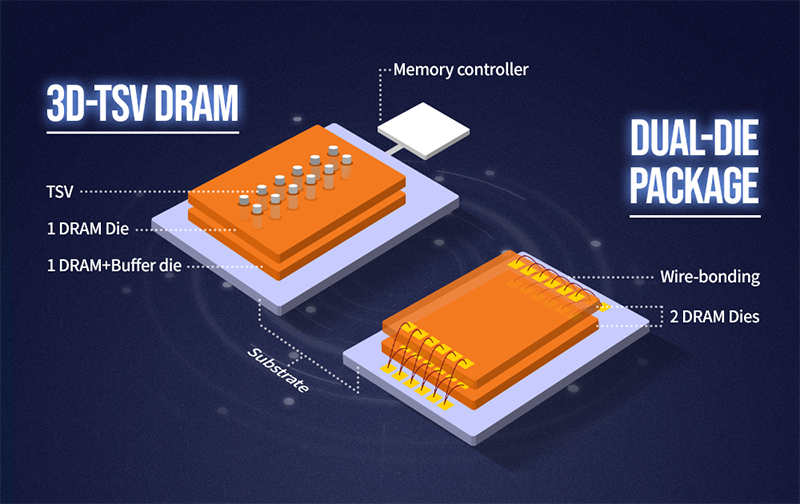
Through-Silicon-Via (TSV) in memories has emerged as an efficient foundational technology for capacity expansion and bandwidth extension. It is a technology where vias are perforated through the entire silicon wafer thickness, in order to form thousands of vertical interconnections from the front to the back-side of the die and vice versa. In the earlier days, TSV was regarded merely as a packaging technology, simply replacing wire-bondings. But over the years, it has become an essential tool to scale performance and density of DRAMs. Today, there are two main use cases in the DRAM industry, where TSVs have been successfully productized to overcome capacity and bandwidth scaling limitations. These are 3D-TSV DRAM and High-Bandwidth-Memory (HBM).
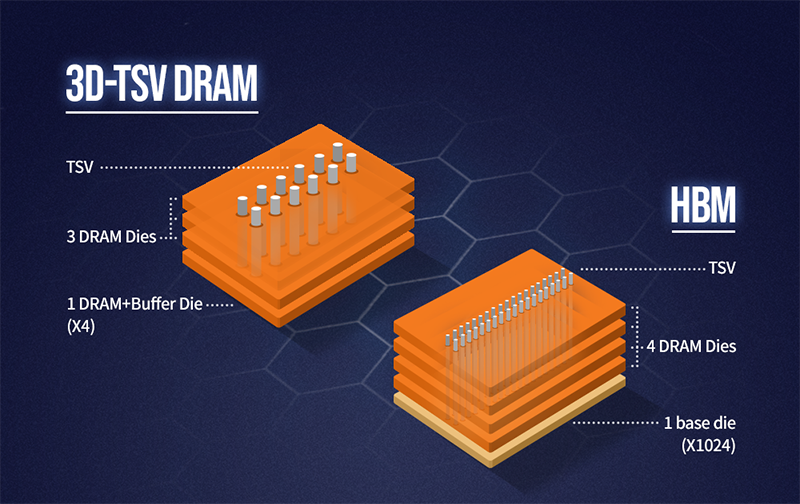
High density memories such as 128 and 256GB DIMMs (16Gb based 2rank DIMMs with 2High and 4High X4 DRAMs) are also adopting 3D-TSV DRAMs in addition to traditional Dual-Die-Packages (DDP) having wire-bonded die stacks. In 3D-TSV DRAMs, 2 or 4 DRAM dies are stacked on top of each other, where only the bottommost die is connected externally to the memory controller. The remaining dies are interconnected through many TSVs internally providing Input/Output (I/O) load isolations. Compared to DDP structures, such architecture allows higher pin speeds through decoupling of I/O loadings, and lower power consumption by eliminating unnecessary duplication of circuit components across the stacked dies.
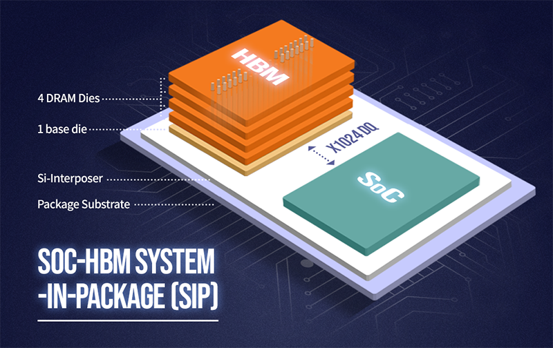
On the other hand, HBM has been primarily created to bridge the bandwidth gap between the system- on-a-chip (SoC) high bandwidth demands and maximum bandwidth supply capabilities of main memories. For example, in AI applications, bandwidth demands per SoC, particularly in training applications, can exceed a few TB/s which cannot be satisfied with conventional main memories. A single main memory channel with 3200Mbps DDR4 DIMMs can provide only 25.6GB/s bandwidth. Even the most advanced CPU platforms with 8 memory channels can provide only 204.8GB/s. On the other hand, 4 HBM2 stacks around a single SoC can provide >1TB/s bandwidth, capable of bridging their bandwidth gaps. Depending on applications, HBMs can be used either stand-alone, as a cache or as the first tier in a two-tier memory.
HBM is an in-package memory where it is integrated with a SoC through a silicon interposer inside the same package. This allows it to overcome the maximum number of data I/O package pin limitations, which would otherwise exist in conventional off-chip packages. HBM2, which has already been deployed in actual products, consists of 4 or 8-high stacks of 8Gb dies and 1024 data pins running at 1.6~2.4Gbps each. This results in 4 or 8GB density and 204~307GB/s bandwidth per HBM stack.
SK hynix has always been committed to maintaining industry leadership in both HBM and high-density 3D-TSV DRAM products. Recently, SK hynix announced the successful development of the HBM2E device, an extended version of HBM2, which reaches higher density of up to 16GB and bandwidth of 460GB/s per stack. This was made possible through the increase of DRAM die density to 16Gb and achieving 3.6Gbps per pin speed over 1024 data IOs at 1.2V supply voltage. SK hynix is also in the process of expanding line-ups of 128~256GB 3D-TSV DIMMs to satisfy the needs of its customers for higher density DIMMs.
TSV technology has now reached its maturity to some extent, being able to build state-of-the-art products such as HBM2Es with thousands of TSVs. In the future, however, decreasing the TSV pitch1/diameter/aspect-ratio2 and the die thickness, while still maintaining high assembly yields, will become more challenging and essential for continued future device performance and capacity scaling. Such improvements will allow decreased TSV loadings, reduced TSV relative die size portions, and the extended number of stacks beyond 12Highs while still maintaining the same total physical stack height. SK hynix will continue to be dedicated to positioning itself at the forefront of memory technology leadership through endless innovations in TSV products and technology.

By Uksong Kang
Vice President and Head of DRAM Product Planning at SK hynix