The SK hynix Newsroom is running a series of interviews with the Top Team—the executives in charge of the company’s major business divisions. This series provides insights into the business strategies, organizational culture, and more promoted by the leaders to achieve the company’s vision. For this latest interview, the newsroom spoke with Vice President and Head of Package & Test (P&T) Woojin Choi.

For the past 30 years, Woojin Choi has conducted and led R&D in semiconductor memory packaging. During that time, packaging has become increasingly important and is now a pivotal technology for in-demand AI memory solutions such as HBM1.
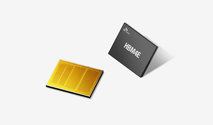
1High Bandwidth Memory (HBM): A high-value, high-performance product that revolutionizes data processing speeds by connecting multiple DRAM chips with through-silicon via (TSV).
As the technology environment has evolved, packaging has become a game-changer in the AI memory market. Amidst this backdrop, Choi, who was appointed as head of SK hynix’s Package & Test (P&T) at the end of 2023, is determined to prove the company’s technological edge. In this latest Top Team Insights interview, the newsroom spoke with Choi about the importance of packaging technologies in the AI era, taking on new challenges, and his mission to go “beyond HBM”.
Leading the AI Memory Market through Limitless Challenges
After wafers undergo the semiconductor front-end process in fabs, P&T oversees the back-end process where wafers are packaged into products and tested to ensure they meet customer expectations.
While packaging traditionally held the role of electrically connecting chips and protecting them from external shocks, it is now vital to enabling differentiated product performances. Consequently, advanced packaging technologies such as TSV2 and MR-MUF3 have grown in importance as they have proven to be critical in the development of key products including HBM.
2Through-silicon via (TSV): A technology that drills microscopic holes in DRAM chips to vertically connect silicon dies through electrodes.
3Mass Reflow-Molded Underfill (MR-MUF): Mass reflow is a technology that connects chips together by melting the bumps between stacked chips. Molded underfill fills the gaps between stacked chips with protective material to increase durability and heat dissipation.

Choi believes that facing new challenges will enable a company to become an industry leader in the AI era
“P&T technology is turning into a crucial factor in the battle for semiconductor leadership,” Choi claimed. “As demand for high-performance chips is exploding in the AI era, we will contribute to the development of the highest-performance memory products through advanced packaging technologies.
Choi emphasizes to his employees the importance of setting no limits to challenges. “The way we have aggressively taken on tough challenges has lifted the Korean semiconductor industry to where it is today,” he said. “At a time when countries around the world are investing huge amounts of capital to secure leadership in the semiconductor market, it has become even more vital to continuously embrace new challenges.”
According to Choi, the global semiconductor race has even been likened to a war due to its intense environment. “If continuous innovations and efforts to overcome challenges cease, it could be disastrous for a company,” he said. “It is more crucial than ever to push the limits in all areas of product development including performance, yield, and cost competitiveness.”

Choi says that advanced packaging technologies are key to developing next-generation signature memories
As AI memory is a key pillar in the global semiconductor race, Choi presented the development of signature memories as a key strategy to revolutionize this technology.
“In the age of AI, SK hynix is focusing on signature memories which possess diverse aspects required by customers, including various capabilities, sizes, shapes and power efficiency,” Choi explained. “To realize these products, we are advancing technologies such as TSV and MR-MUF which play a key role in HBM performance. Moreover, we are developing various next-generation packaging technologies including chiplet4 and hybrid bonding5. These innovations will contribute to the development of new types of semiconductors while supporting heterogeneous integrations such as between semiconductor memory and logic chips.”
4Chiplet: A technology that breaks up chips into functions and connects these separated pieces called chiplets on a single substrate to enable heterogeneous bonding and integration.
5Hybrid Bonding: A technology that connects chips together directly without bumps to enable higher bandwidth and capacity. This allows for shorter data pathways and the ability to stack more chips in the same space.
Choi stresses that his department will not limit themselves when taking on challenges and will demonstrate their strong technological advantage.
The Next Innovation and Challenge: Building a Global Manufacturing Base
Choi’s emphasis on challenges makes sense when looking at his career. In 2020, he succeeded in developing a heat dissipation solution for HBM3 to improve the product’s performance. He also helped tackle the industry downturn in 2023 by reducing costs in areas including materials and general expenses. Additionally, he quickly secured a production line to meet the growing demand for DRAMs during the rapid rise of ChatGPT, helping SK hynix strengthen its leadership in AI memory.
“It was challenging to respond immediately to the sudden surging demand for AI memory in 2023, but we quickly utilized our TSV packaging line with no additional investments to ramp up the production of our server-oriented 3D stacked memory (3DS)6 modules based on DDR5 DRAM,” Choi recalled. “This is an example of a bold decision made in a short period of time. We would not have been able to accomplish this feat if we had hesitated.”
63D Stacked Memory (3DS): A high-bandwidth memory product that is packaged by connecting two or more DRAM chips through TSV. 3DS and HBM differ in that the latter is supplied to the system company before packaging is completed, and it is then packaged with logic chips such as GPUs.

Choi has an instrumental role in the planning of SK hynix’s new manufacturing facility in Indiana
Now, Choi’s challenge awaits overseas. On April 3, SK hynix announced plans to establish a packaging manufacturing facility in the U.S. state of Indiana to enhance its competitiveness in the global HBM market while also enhancing its R&D capabilities in advanced packaging.
Choi is playing a key role in this process by planning the strategy for the construction and operations of the fab. The U.S. packaging plant will receive HBM wafers that have undergone the front-end process from the Korean HQ to produce finished products and, at the same time, actively cooperate in R&D with global companies.
“We are currently in the process of refining the fab design and mass production system, as well as preparing to build an R&D cooperation ecosystem with global companies,” Choi explained. “Once the factory is fully operational, we expect it to make a significant contribution to strengthening the company’s AI memory technology and business leadership.”
Going “Beyond HBM”: Data-Centric Innovations and Focus on Employee Development
As for the important missions of P&T, Choi mentioned maximizing profitability and what he calls going “beyond HBM.” “In the short term, we plan to strengthen our domestic production capabilities to meet demand for HBM while leveraging our global base to maximize profitability,” he said. “In the long run, we aim to secure more innovative packaging technologies like MR-MUF, which is now a vital technology to HBM.”
To accomplish this, Choi highlights the significance of finding answers in the data, a philosophy he has followed throughout his decades of experience in the packaging field.
“As there is a tremendous amount of data during the P&T process, the saying that the ‘answer is in the data’ proves to be true,” Choi said. “If we utilize this data well, we can improve yields and even find clues for new product development. We need to work with the idea that data can guide us to growth.”

To go “beyond HBM,” Choi emphasizes utilizing data for growth and focusing on membership development
Lastly, Choi underlined his commitment to supporting the growth of SK hynix employees. “It is our members who have raised the profile of packaging technology,” he said. “Many of the breakthroughs we have made, such as solving the heat dissipation issue of HBM at the packaging stage, have come from their ideas.” Accordingly, Choi plans to lay the foundation for continued growth so employees can always take on challenges with the mindset of leading the global market.
“Our company is actively interacting with universities and research institutes at home and abroad,” he added. “We plan to capitalize on this to help P&T members gain diverse global experiences and further improve their R&D capabilities to aid their growth and development.”